System and method for testing parasitic inductance

A test system and parasitic inductance technology, applied in the direction of measuring electrical variables, measuring resistance/reactance/impedance, measuring devices, etc., can solve problems such as IGBT damage, achieve optimal reliability and reduce design costs

Inactive Publication Date: 2012-06-13
DELTA ELECTRONICS SHANGHAI CO LTD +1
View PDF7 Cites 15 Cited by
  • Summary
  • Abstract
  • Description
  • Claims
  • Application Information

AI Technical Summary

Problems solved by technology

It is not difficult to see that once the voltage superimposed on both ends of the IGBT e

Method used


Image

  • System and method for testing parasitic inductance
  • System and method for testing parasitic inductance
  • System and method for testing parasitic inductance

Examples


Embodiment Construction

[0038] In order to make the technical content disclosed in this application more detailed and complete, reference may be made to the drawings and the following various specific embodiments of the present invention, and the same symbols in the drawings represent the same or similar components. However, those skilled in the art should understand that the examples provided below are not intended to limit the scope of the present invention. In addition, the drawings are only for schematic illustration and are not drawn according to their original scale.

[0039] The specific implementation manners of various aspects of the present invention will be further described in detail below with reference to the accompanying drawings.

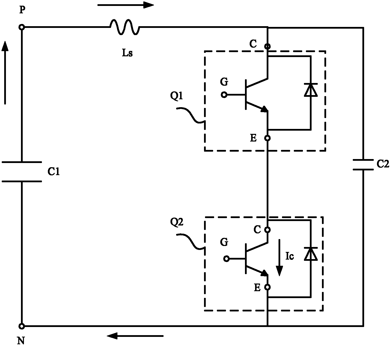
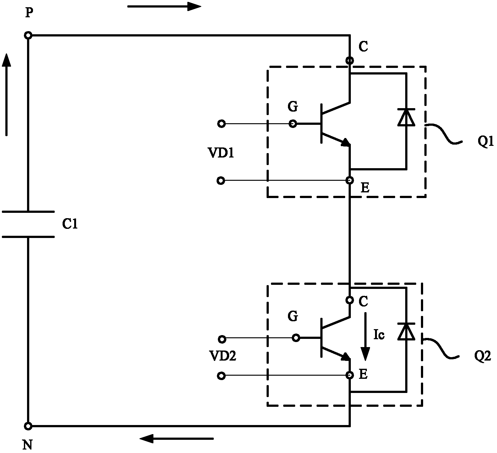
[0040] figure 1 Shows the parasitic inductance L in the inverter main circuit S Schematic of the snubber circuit. refer to figure 1 , the inductance L on the DC bus of the inverter main circuit S Equivalently expressed as the parasitic inductance in th...


PUM


Abstract

The invention provides a system and a method for testing a parasitic inductance value. The system comprises a circuit to be tested, a driving device and a test device, wherein a direct current source supplies power to an inversion bridge arm of the circuit to be tested; the driving device is electrically connected to a control electrode of each switch body in the inversion bridge arm; the test device is used for testing an inversion bridge arm voltage which is carried by a switch body to be tested in the inversion bridge arm during instant turning-off and the change rate of a current which flows through the inversion bridge arm; and according to voltages of the switch body and the direct current source and the change rate of the current which flows through the inversion bridge arm, the parasitic inductance value is obtained by calculation. By adoption of the invention, under the control of the driving device, an upper bridge arm switch body keeps turned on, and a lower bridge arm switch body is turned on and turned off; and the test device tests a bridge arm voltage which is carried by the lower bridge arm switch body and the change rate of the current which flows through the lower bridge arm switch body, the parasitic inductance value is obtained by calculation, and quantization basis is provided for selection of design parameters of an absorption circuit, so that the reliability of an inverter is optimized, and the design cost of a product can be reduced.

Description

technical field [0001] The present invention relates to parasitic inductance in inverter circuits, and more particularly to a system and method for testing the parasitic inductance. Background technique [0002] Currently, in the main circuit of the inverter, the surge voltage of the power bus mainly includes the turn-off surge voltage of the IGBT and the recovery surge voltage of the freewheeling diode. The main reason for these surge voltages is that there are inevitably parasitic inductances in the main circuit of the inverter, such as the parasitic inductance of the DC bus, the parasitic inductance inside the power device, and the parasitic inductance presented when the power device leads. When the power device commutates in the power loop under the action of the drive circuit, the current flowing through the parasitic inductance will change suddenly, so the parasitic inductance generates a voltage (also called parasitic electromotive force) that prevents the current fro...

Claims


Application Information

Patent Timeline
IPC IPC(8): G01R27/26
Inventor 董文鹏党彦明
Owner DELTA ELECTRONICS SHANGHAI CO LTD
Why Eureka
Try Eureka