Spike timing activity conversion circuit

A technology of pulse timing and conversion circuit, applied in information storage, static memory, digital memory information and other directions, can solve the problems of low power consumption, low integration, complex circuit structure, etc.

Active Publication Date: 2012-06-13
UNIV OF ELECTRONICS SCI & TECH OF CHINA
View PDF4 Cites 22 Cited by
  • Summary
  • Abstract
  • Description
  • Claims
  • Application Information

AI Technical Summary

Problems solved by technology

[0005] At present, most of the weight adjustment circuit structures based on STDP learning rules are designed for simulating synapses with MOS circuits, which have complex structures and low integration
In recent years, a new type of electronic synapse structure has been proposed, that is, a resistive variable memory is used to simulate a synapse. However, there are still few specific weight adjustment circuits based on STDP learning rules for RRAM analog synapses.

Method used


Image

  • Spike timing activity conversion circuit
  • Spike timing activity conversion circuit
  • Spike timing activity conversion circuit

Examples


Embodiment Construction

[0023] The specific implementation manner of the present invention will be further described in detail below in conjunction with the accompanying drawings and specific examples.

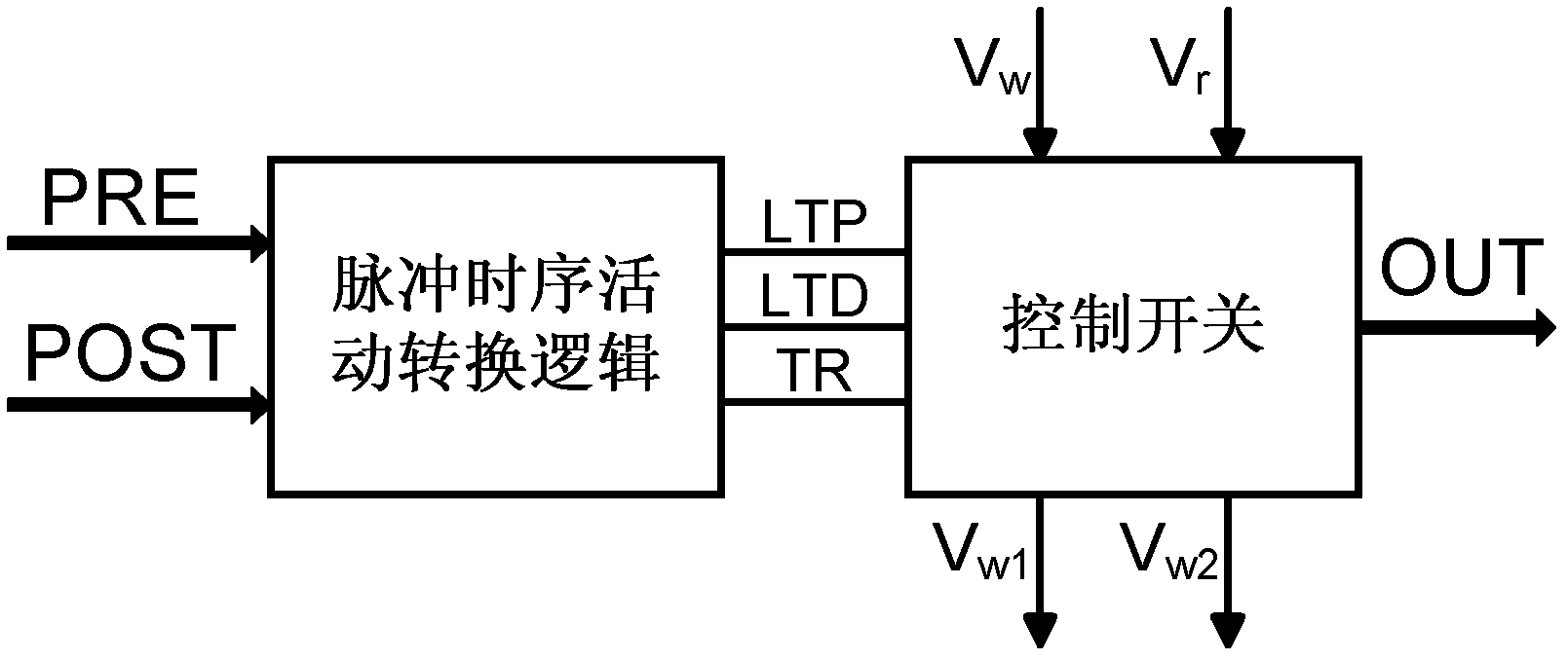
[0024] like Figure 3A Shown is the structural block diagram of the pulse timing activity conversion circuit, Figure 3B A schematic diagram of the overall package structure of the circuit is shown. PRE and POST are two input terminals in the pulse timing activity conversion circuit, which are used to receive two pulse signals to be converted into pulse timing activity (pre-synaptic neuron and synapse when used as a synaptic weight adjustment circuit) impulse signal sent by post-synaptic neurons); V w and V r The operating voltage is provided to the pulse timing activity conversion circuit (when used as a synaptic weight adjustment circuit, it is used as a write operation voltage for a resistive variable memory and a read operation voltage for a weight when a signal is transmitted).

[0025] like...


PUM


Abstract

The invention relates to a principle about the connection among neurons in neural networks in integrated circuits and biology. A spike timing activity conversion circuit is composed of spike timing activity conversion logic and a control switch. The spike timing activity conversion logic receives a signal (PRE) and a signal (POST) which are treated to generate a long term potentiation (LTP) signal, a long term depression (LTD) signal or a transmission control (TR) signal. The three signals are output to the control switch, which is in connection with write operation voltage (Vw) and read operation voltage (Vr) of a resistive synapse. Under the control of the TR, LTP and LTD signals, output (OUT) of transinformation can be generated, or proper voltage can be output to Vw1 and Vw2 which are voltages respectively added to the two ends of the resistive synapse. The invention provides a conversion circuit, which can convert a spike timing activity relation into corresponding LTP and LTD spikes for output according to an STDP (spike timing dependent plasticity) rule, thus realizing the function of an STDP model. Therefore, the conversion circuit can be conveniently applied in neural networks, electronic synaptic weight adjustment and other circuits.

Description

technical field [0001] The invention belongs to the field of integrated circuits, and in particular relates to a pulse sequence activity conversion circuit, which can be used to perform STDP weight adjustment operations on electronic synapses based on resistive memory, and realize the memory and self-simulation of human brain neural networks in the form of circuits. learning function. technical background [0002] Since the birth of computers, human beings have longed for a day when computers, like human brains, have self-learning ability, can solve problems by themselves, and become computers with real artificial intelligence. Traditional computers use the von Neumann architecture, which is good at mathematical and logical calculation processing, but lacks self-learning and self-adaptation capabilities, and often feels powerless in dealing with problems such as associative memory and image thinking. In contrast, the human brain is capable of self-learning and self-adaptati...

Claims


Application Information

Patent Timeline
Patent Type & Authority Applications(China)
IPC IPC(8): G11C11/56G11C11/4193
Inventor 刘洋吴洪天于奇胡绍刚
Owner UNIV OF ELECTRONICS SCI & TECH OF CHINA
Why Eureka
Try Eureka