Design and preparation method of non-refrigeration infrared detector

An uncooled infrared and detector technology, applied in semiconductor devices, radiation control devices, final product manufacturing, etc., can solve the incompatibility of silicon micromachining technology, limit the miniaturization and integration of infrared detectors, detection sensitivity, and response speed Limited problems, to achieve the effect of convenient circuit design, low cost and high sensitivity

Inactive Publication Date: 2012-06-20
PEKING UNIV
View PDF6 Cites 20 Cited by
  • Summary
  • Abstract
  • Description
  • Claims
  • Application Information

AI Technical Summary

Benefits of technology

This patented device includes two main technical features - one being its ability to operate evenly over multiple wavelengths without refrigerating or requiring expensive components like cooling systems; another being able to sense very small amounts (<2 mm) of light accurately due to this unique property called pn junction's thermopic response curve.

Problems solved by technology

Technological Problems addressed in this patents include improving thermosensitive elements like bolziters, quantum well diodes, crystal lattice structures, and opaque metal films. These technical problem areas involve developing smaller devices while maintaining their performance capabilities during extreme environments including those associated with infrainfeldray shielding functions.

Method used


Image

  • Design and preparation method of non-refrigeration infrared detector
  • Design and preparation method of non-refrigeration infrared detector
  • Design and preparation method of non-refrigeration infrared detector

Examples


specific example

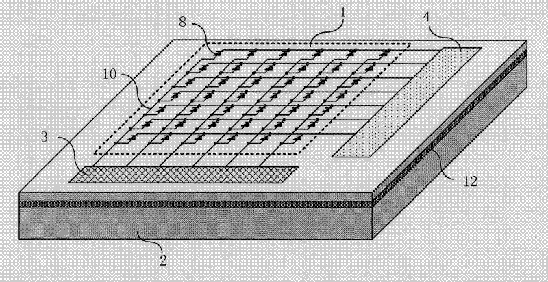
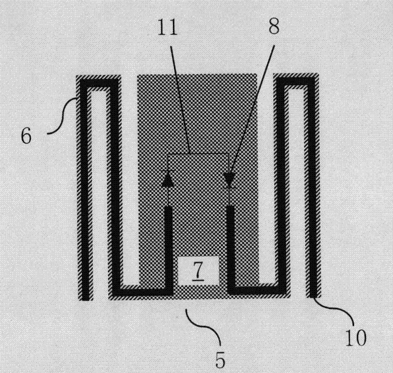
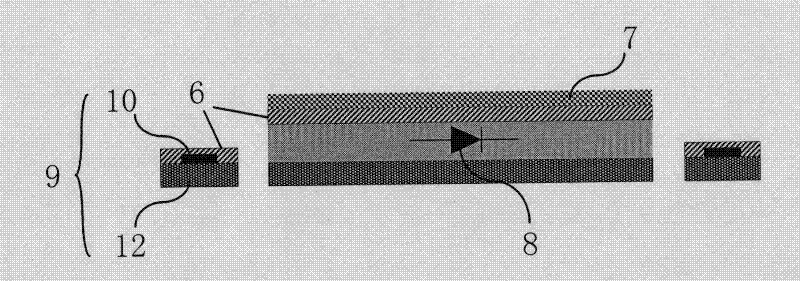
[0068] 1) The SOI substrate is used as the processing substrate, and the thickness of the device layer is Buried oxide layer thickness The thickness of the Si substrate is 525 μm. The first photolithography, the photoresist is used as a mask, and the device layer Si is etched to form a PN junction active region;

[0069] 2) The thickness of low pressure chemical vapor deposition is SiO 2 , perform boron ion implantation on the front side of the substrate, the implantation energy is 50KeV, and the implantation concentration is 1×10 13 / cm 3 , annealing at 1050°C for 4 hours, so that the implanted B ions diffuse uniformly in the device layer to form the P region of the PN junction;

[0070] 3) For the second photolithography, the photoresist is used as a mask, the N region of the PN junction is patterned, and phosphorus ions are implanted. The implantation energy is 80KeV, and the implantation concentration is 1×10 15 / cm 3 , wet etching removes step 2) the electrogene...


PUM

PropertyMeasurementUnit
Areaaaaaaaaaaa

Abstract

The invention discloses a design and preparation method of a non-refrigeration infrared detector, in particular to the design and preparation of a multi-band non-refrigeration infrared detector based on monocrystalline silicon PN junction temperature characteristics. The infrared detector provided by the invention consists of an infrared focal plane array, a substrate and a driving and reading circuit, wherein the substrate supports the focal plane array, the driving and reading circuit is positioned on the substrate, the PN junction is used as a temperature sensing unit in the infrared detector to be arranged in a pixel element of the focal plane array, the absorbed heat energy is converted into voltage signals to be output, an infrared absorption structural layer arranged on the pixel element is used for realizing the absorption of infrared radiation in different wave bands, and the focal plane array signals are finally output by a reading circuit. The infrared detector provided by the invention can realize the non-refrigeration work and the multi-wave-band infrared detection.

Description


Claims


Application Information

Patent Timeline
Owner PEKING UNIV
Why Eureka
Try Eureka