Supercharge Your Innovation With Domain-Expert AI Agents!

Process for recycling photodiode

A photodiode and process technology, applied in circuits, electrical components, semiconductor devices, etc., can solve the problems of easily damaged PD lenses and gold layers, and achieve the effect of improving recovery yield and easy removal

Active Publication Date: 2014-03-12
SOURCE PHOTONICS CHENGDU
View PDF3 Cites 0 Cited by
  • Summary
  • Abstract
  • Description
  • Claims
  • Application Information

AI Technical Summary

Problems solved by technology

[0004] The purpose of the present invention is to provide a process for recovering photodiodes, which solves the disadvantages of easily damaging the PD lens and gold layer due to uneven stress when recovering PDs using the existing process, and improves the recovery yield

Method used


Image

  • Process for recycling photodiode
  • Process for recycling photodiode
  • Process for recycling photodiode

Examples


Embodiment Construction

[0024] The technical solutions in the embodiments of the present invention will be clearly and completely described below in conjunction with the accompanying drawings in the embodiments of the present invention. Obviously, the described embodiments are only a part of the embodiments of the present invention, rather than all the embodiments. Based on the embodiments of the present invention, all other embodiments obtained by those of ordinary skill in the art without creative work shall fall within the protection scope of the present invention.

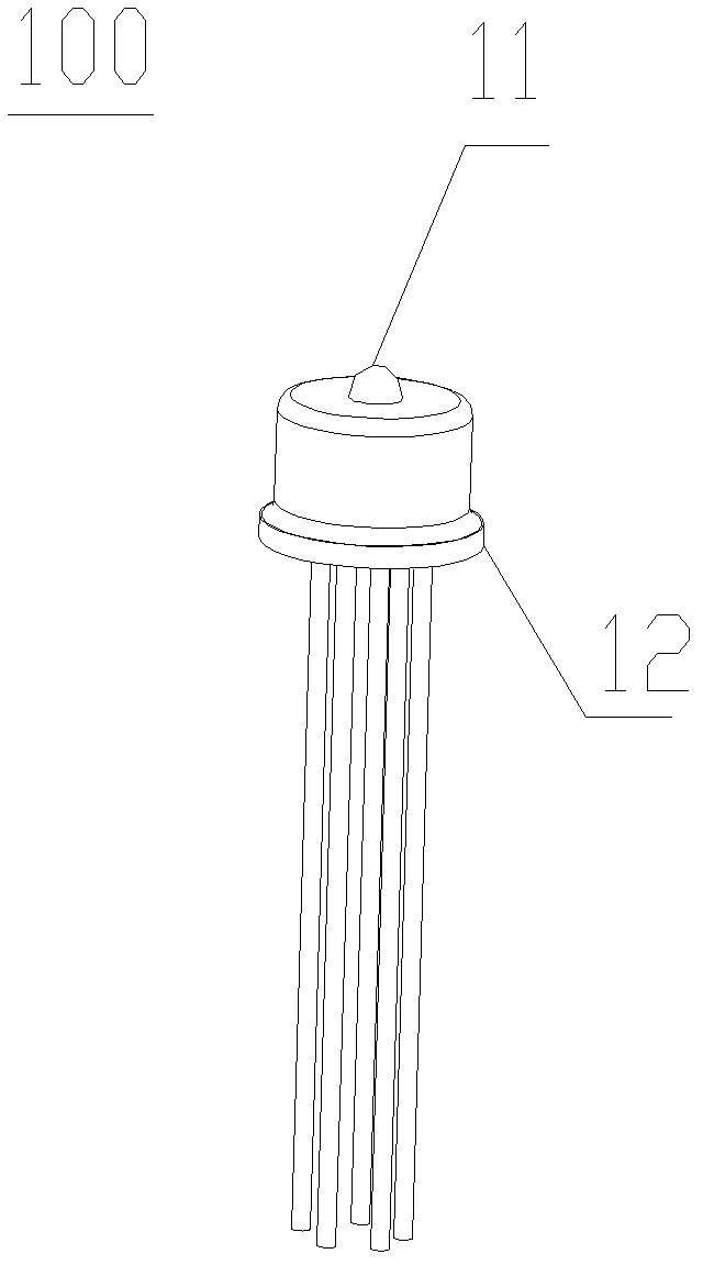
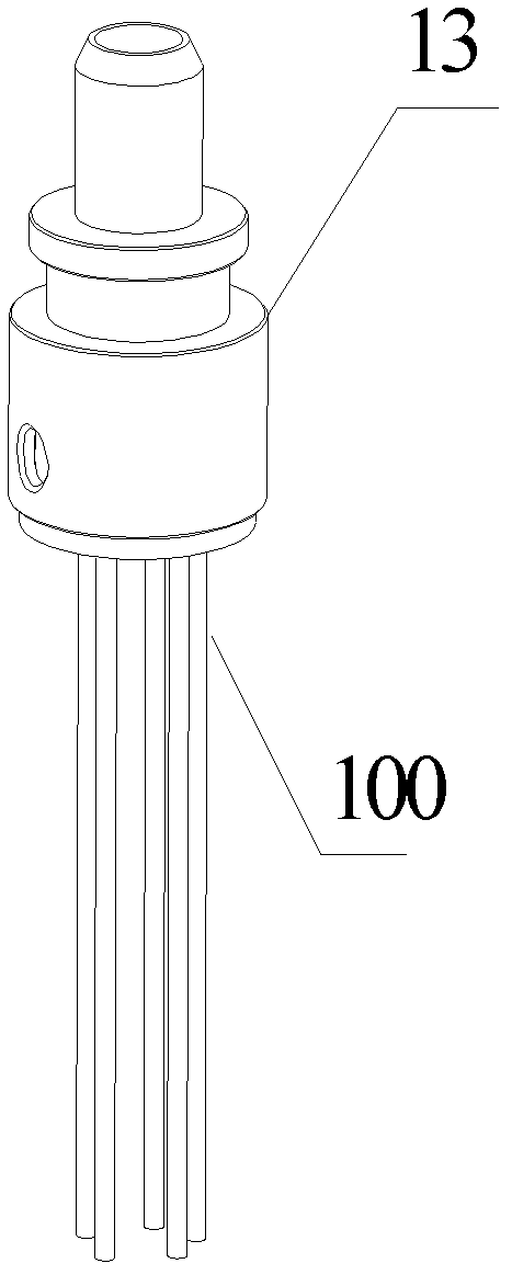
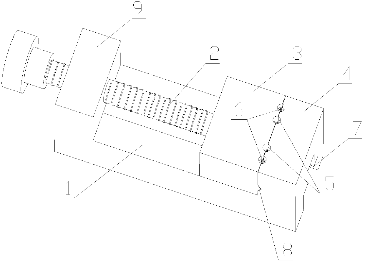
[0025] The process of recycling photodiodes in the embodiment of the present invention is mainly used to recover photodiodes from the light receiving sub-module ROSA. The process uses flat-nose pliers with fixing holes and diagonal pliers with clamping holes, for better explanation The process proposed by the present invention will firstly describe the tools used in the process.

[0026] See image 3 , Figure 4 , Is a schematic diagram of...


PUM


Abstract

The invention discloses a process for recycling a photodiode, which is used for recycling the photodiode from a light receiving sub-module ROSA, and adopting a pair of flat tongs with a fixing hole and a pair of diagonal pliers with a clamping hole to place the ROSA to be recycled in the fixing hole of the flat tongs for fixing and enabling ROSA golden layers to be exposed out of the fixing hole of the flat tongs. The diagonal pliers with the clamping hole is used for clamping black glue at the lower end of the ROSA golden layer, and slight left-and-right prying is performed until the photodiode is loosened and disassembled. When the photodiode (PD) is recycled from the ROSA by utilizing the process, the ROSA can be fixed in the fixing hole on the flat tongs, the diagonal pliers can be used for clamping a lens of the PD and an inner circle between the golden layers, the whole disassembling process is performed through face contact, uneven stress distribution does not exist basically, the complete PD can be fetched out easily, and recycling yield is improved.

Description

Technical field [0001] The invention relates to the field of industrial recycling, in particular to a process for recycling photodiodes. Background technique [0002] Photo-diode (PD, Photo-Diode), like ordinary diodes, is a semiconductor device composed of PN junctions and has unidirectional conductivity. However, it is not used as a rectifier element in the circuit, but is a photoelectric device that converts optical signals into electrical signals. Sensor device, its specific structure can be found in figure 1 . The core cost of optical devices is mainly composed of PD and LD (Semiconductor Laser, Laser Diode), and in the entire optical communication production industry, most of them are semi-automated production, so the direct rate of products is often not high, and many products need to be reworked. To save costs, PD will generally be recycled based on the reasons for poor production. The Receiver Optical Subassembly (ROSA, Receiver Optical Subassembly) is composed of the ...

Claims


Application Information

Patent Timeline
Patent Type & Authority Patents(China)
IPC IPC(8): H01L31/18
Inventor 杨帅田英俊
Owner SOURCE PHOTONICS CHENGDU
Features
  • R&D
  • Intellectual Property
  • Life Sciences
  • Materials
  • Tech Scout
  • Unparalleled Data Quality
  • Higher Quality Content
  • 60% Fewer Hallucinations
Learn More