Solder resist manufacturing method of thick copper plate

A production method and technology for thick copper plates, which are used in the solder mask production of thick copper plates. In the field of solder mask production of 4OZ PCB boards, it can solve the problems of inconsistent thickness of line and corner ink, and achieve uniformity and consistency, and increase the thickness. Effect

Inactive Publication Date: 2013-12-04
SHENZHEN SUNTAK MULTILAYER PCB
View PDF1 Cites 0 Cited by
  • Summary
  • Abstract
  • Description
  • Claims
  • Application Information

AI Technical Summary

Problems solved by technology

[0004] For this reason, the purpose of the present invention is to provide a method for manufacturing thick copper plate solder resist, to solve the problem that the thickness of the ink on the surface of the circuit board and the ink thickness of the line corners are not consistent with the current production of thick copper plate solder resist by secondary screen printing or spraying.

Method used


Image

  • Solder resist manufacturing method of thick copper plate
  • Solder resist manufacturing method of thick copper plate
  • Solder resist manufacturing method of thick copper plate

Examples


Embodiment Construction

[0022] In order to illustrate the idea and purpose of the present invention, the present invention will be further described below in conjunction with the accompanying drawings and specific embodiments.

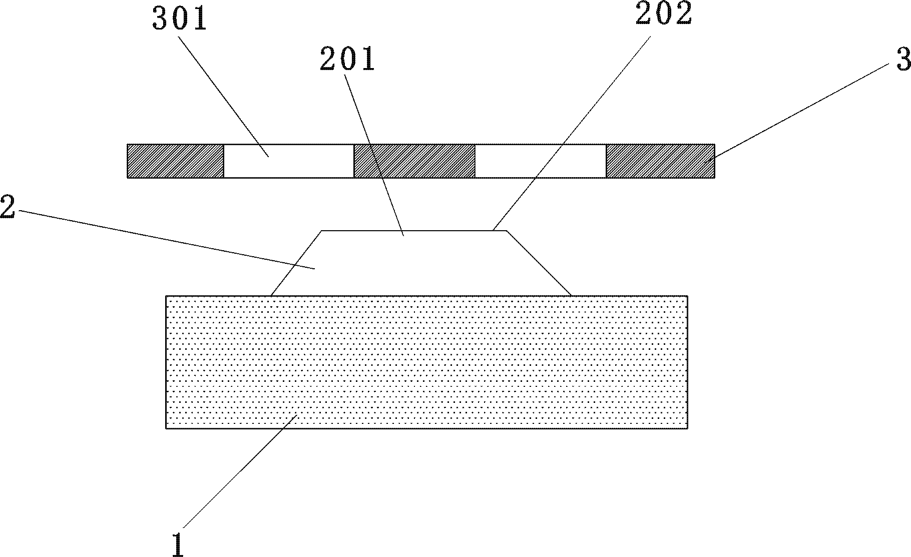
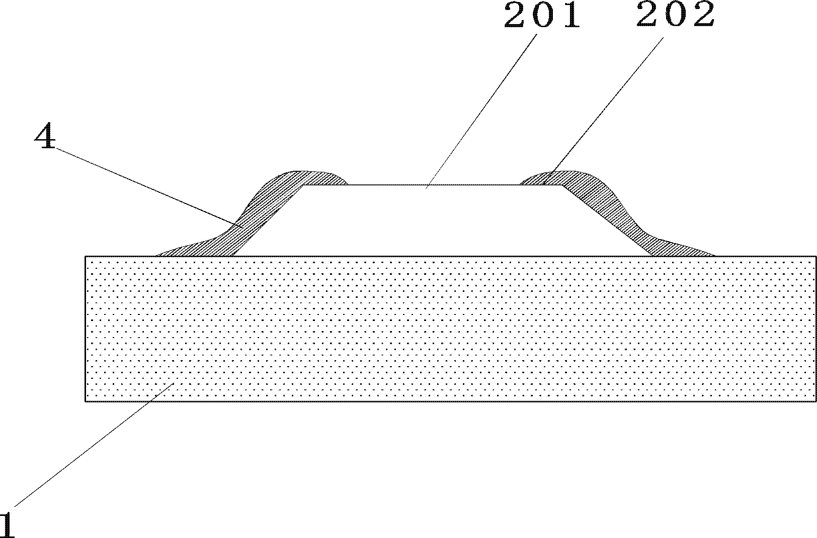
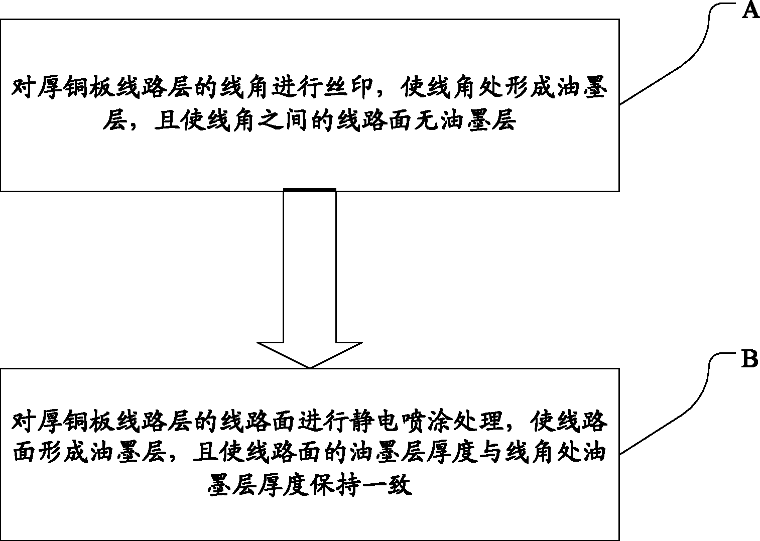
[0023] The present invention provides a method for manufacturing thick copper plate solder resist, which solves the problem of circuit boards existing in the current production of thick copper plate solder resist by secondary silk screen printing or spraying by performing silk screen printing on the line corners first, and then performing silk screen printing on the circuit surface The problem that the surface ink thickness is inconsistent with the line corner ink thickness.

[0024] See figure 1 , figure 2 as shown, figure 1 It is a schematic cross-sectional structure diagram of the circuit board of the present invention carrying out line angle screen printing through a screen; figure 2 It is a schematic diagram of the screen printing effect of the line corner of the ci...


PUM


Abstract

The invention discloses a solder resist manufacturing method of a thick copper plate, comprising the following steps of: A, carrying out silk-screen printing on line angles of a thick copper plate circuit layer to form oil ink layers at the line angles and not form the oil ink layer on a circuit surface between the line angles; and B, carrying out electrostatic spraying treatment on the circuit surface of the thick copper plate circuit layer to form the oil ink layer on the circuit surface and keep the thickness of the oil ink layer on the circuit surface the same as that of the oil ink layers at the line angles. Compared with the prior art, the solder resist manufacturing method of the thick copper plate solves the problem that the thickness of the oil ink layer on a board surface of a circuit board, which is formed by secondary silk-screen printing or spraying, is not the same as the thickness of oil ink of the line angles; the thickness of the oil ink of the line angles is further increased while the thickness of the oil ink on a copper surface is ensured, so that the uniformity and the consistency of the thickness of the oil ink of the circuit layer are ensured.

Description

Technical field: [0001] The invention belongs to the technical field of PCB manufacturing, and in particular relates to a method for manufacturing thick copper boards with solder resistance, in particular to PCB boards with a surface copper foil thickness greater than or equal to 4OZ. Background technique: [0002] The solder mask production of PCB thick copper board is related to the thickness of the surface copper foil, especially when the surface copper foil thickness is greater than or equal to 4OZ, when the PCB board solder mask is produced, it is easy to have ink thickness not up to standard, vertical flow, false copper exposure and Problems such as air bubbles, in order to solve such problems in the industry, the method of secondary screen printing or spraying is usually used, and the ink with a slightly thinner viscosity and the screen with a larger mesh number are selected each time, and the first printing oil is pre-baked About 10 minutes less than usual. [0003]...

Claims


Application Information

Patent Timeline
Patent Type & Authority Patents(China)
IPC IPC(8): H05K3/28
Inventor 荣孝强彭卫红朱拓魏秀云
Owner SHENZHEN SUNTAK MULTILAYER PCB
Why Eureka
Try Eureka