Method for manufacturing PCB (Printed Circuit Board), PCB and electronic equipment

A technology of electronic equipment and manufacturing method, which is applied in the direction of printed circuit manufacturing, printed circuit, printed circuit, etc., and can solve the problems of laser head wear and high processing cost

Inactive Publication Date: 2012-07-04
HUAWEI DEVICE CO LTD
View PDF3 Cites 13 Cited by
  • Summary
  • Abstract
  • Description
  • Claims
  • Application Information

AI Technical Summary

Problems solved by technology

[0008] Due to the need for laser cutting to divide the cavity in the existing technology, the H of the laser needs to be cut is too high, resulting in serious wear of the laser head and high processing costs

Method used


Image

  • Method for manufacturing PCB (Printed Circuit Board), PCB and electronic equipment
  • Method for manufacturing PCB (Printed Circuit Board), PCB and electronic equipment
  • Method for manufacturing PCB (Printed Circuit Board), PCB and electronic equipment

Examples


Embodiment 1

[0026] see figure 2 as well as Figures 3a-3d , the present embodiment provides a method for manufacturing a circuit board, comprising:

[0027] Step 101 , respectively fixing at least two functional modules and a shielding frame on a substrate of a circuit board, wherein the shielding frame is located between the at least two functional modules.

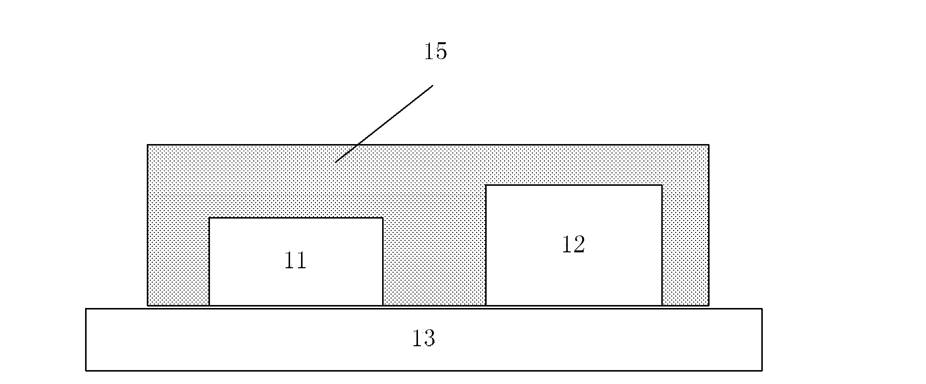
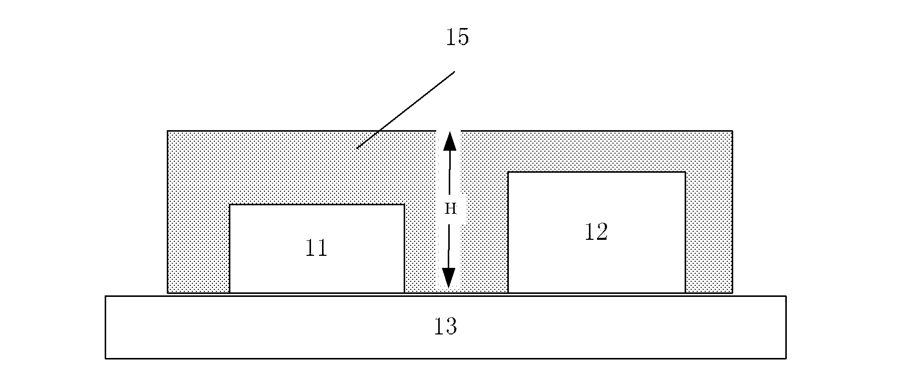
[0028] Take two function modules as an example, see Figure 3a As shown, the functional module 21 , the functional module 22 and the shielding frame 23 are fixed on the substrate 24 of the circuit board, and the shielding frame 23 is located between the functional modules 21 and 22 .

[0029] Step 102: Plastic-encapsulate the at least two functional modules and the shielding frame with a plastic-sealing material to cover the at least two functional modules and the shielding frame.

[0030] see Figure 3b As shown, the functional modules 21 , 22 and the shielding frame 23 are plastic-sealed with a plastic sealing material 25 to ...

Embodiment 2

[0042] see Figure 4 , use the manufacturing method of a kind of circuit board that provides among the embodiment 1 to make mobile phone circuit board in the present embodiment, its method process comprises:

[0043] Step 201. Solder the baseband circuit, the radio frequency circuit and the shielding frame on the substrate of the circuit board respectively, wherein the shielding frame is located between the baseband circuit and the radio frequency circuit.

[0044] In this embodiment, description is made by taking the baseband circuit as the first functional module and the radio frequency circuit as the second functional module as an example, but the first functional module and the second functional module are not limited thereto. For example, SMT can be used to weld the baseband circuit and the radio frequency circuit to the substrate of the PCB. In this embodiment, a shielding frame is welded between the baseband circuit and the radio frequency circuit, and the shielding fra...

Embodiment 3

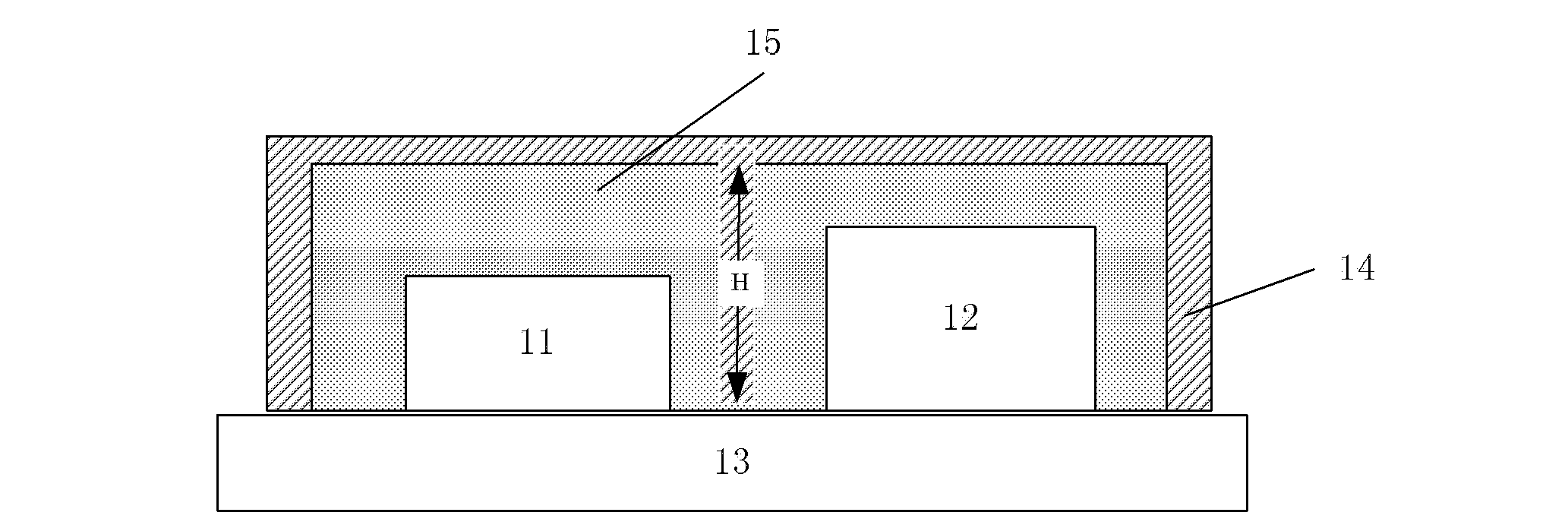
[0058] This embodiment provides a circuit board made using the method provided in Embodiment 1, refer to Figure 3d , the circuit board includes: a substrate 24, at least two functional modules 21, 22, and a shielding frame 23, wherein the at least two functional modules 21, 22, and the shielding frame 23 are fixed to the substrate 24, so The shielding frame 23 is located between the at least two functional modules 21, 22, the sides of the shielding frame 23 and the at least two functional modules 21, 22 are covered by a plastic sealing material 25, and the shielding frame 23 above The outer surface of the plastic sealing material 25 is covered with a conductive material 26 , and the outer surface of the conductive material 26 is covered with an insulating material 27 .

[0059] In this embodiment, the functional modules are all functional modules on the PCB, which may be baseband circuits, radio frequency circuits, antennas, etc., which are not specifically limited in this em...


PUM

PropertyMeasurementUnit
thicknessaaaaaaaaaa

Abstract

The embodiment of the invention discloses a method for manufacturing a PCB (Printed Circuit Board), the PCB and electronic equipment. The method comprises the following steps that: at least two functional modules and a shielding frame are respectively fixed on the PCB, wherein the shielding frame is positioned between the at least two functional modules; the at least two functional modules and the shielding frame can be subjected to plastic package by using a plastic package material; the plastic package material on the shielding frame can be cut to the surface of the shielding frame; and electric conduction material can be covered at the outer surface of the plastic package material and on the shielding frame, and insulation material can be covered at the surface of the electric conduction material. According to the invention, a branch cavity part is shielded by using the shielding frame, other parts comprising edge parts and surface parts of a complete machine are shielded by adopting the electric conduction material, the influence on the size of the whole machine is less, the cutting height is changed into the height formed by directly cutting to the surface of the shielding frame from the original height formed by directly cutting to the surface of the PCB, the height is greatly lowered, the processing time is low, and the good manufacturability is provided.

Description

technical field [0001] The invention relates to a manufacturing method of a circuit board, a circuit board and electronic equipment. Background technique [0002] As the size of electronic components and transistors is getting smaller and smaller, the size of modules, modules, and chips is also getting smaller and smaller. In many packaging forms, highly integrated modules, modules, and chips often integrate baseband circuits, radio frequency circuits, antennas, and other parts. In order to ensure that digital signals, radio frequency signals, and antennas are not interfered with each other, each functional module needs to be shielded in separate chambers. [0003] Such as Figures 1a-1d As shown, in the prior art, the processing flow of sub-cavity shielding by laser cutting and metal spraying is as follows: [0004] a) Using, for example, SMT (Surface Mounted Technology, surface mount technology) to fix (such as soldering) the device 11 and device 12 on the substrate 13 o...

Claims


Application Information

Patent Timeline
Patent Type & Authority Applications(China)
IPC IPC(8): H05K3/30H05K1/18H05K9/00
CPCH05K9/0081H05K9/003H05K3/30H05K3/284H05K3/28H05K2203/107H05K9/0022H05K9/0045H05K2201/2018H05K2201/0715H05K9/00H05K1/0218Y10T29/49124H05K9/0024
Inventor 高春禹
Owner HUAWEI DEVICE CO LTD
Why Eureka
Try Eureka