Supercharge Your Innovation With Domain-Expert AI Agents!

Failure Analysis Methods for Semiconductor Devices

A failure analysis and semiconductor technology, applied in the field of failure analysis of semiconductor devices, can solve problems such as long time consumption, high cost, and solution failure, and achieve the effect of saving time, improving efficiency and success rate

Active Publication Date: 2016-09-14
CSMC TECH FAB2 CO LTD
View PDF8 Cites 0 Cited by
  • Summary
  • Abstract
  • Description
  • Claims
  • Application Information

AI Technical Summary

Problems solved by technology

[0010] However, this solution has the following disadvantages: 1) For high-voltage products, such as 600V DMOS, the contact time between the chip and the acid solution is long, and direct boiling may easily cause the parameters of the semiconductor device to drift, and the semiconductor device cannot be further analyzed. Ineffective; 2) Even if the solution is adopted for low-voltage products, PCCB boards, bonding machines, vinyl, etc. are required in the bonding and packaging process, which is costly, time-consuming, and inefficient

Method used


Image

  • Failure Analysis Methods for Semiconductor Devices
  • Failure Analysis Methods for Semiconductor Devices
  • Failure Analysis Methods for Semiconductor Devices

Examples


Embodiment Construction

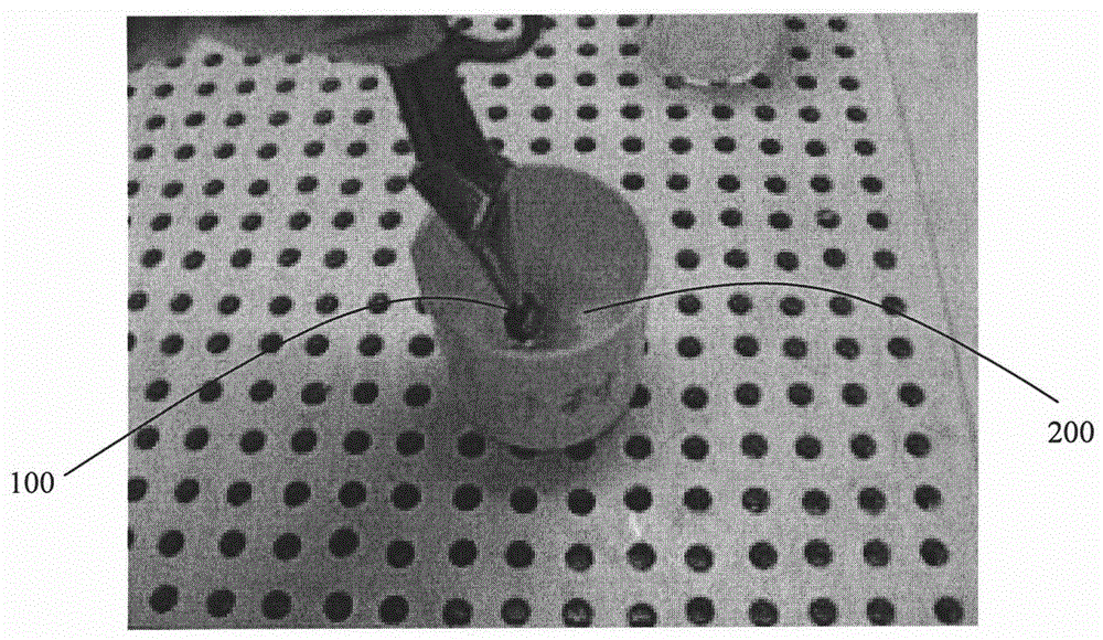
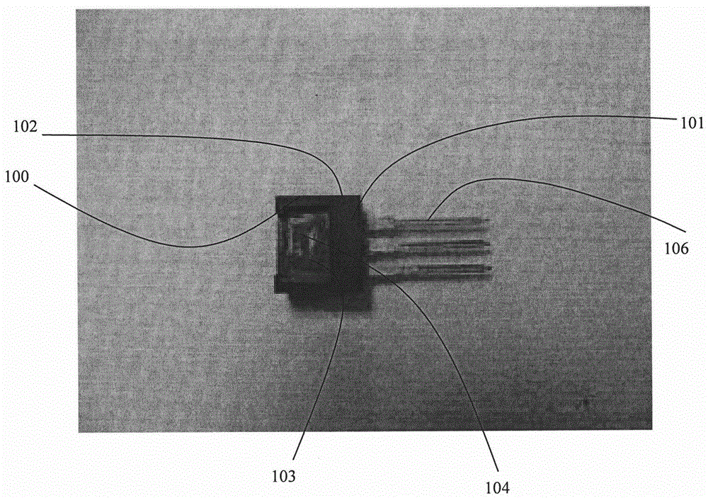
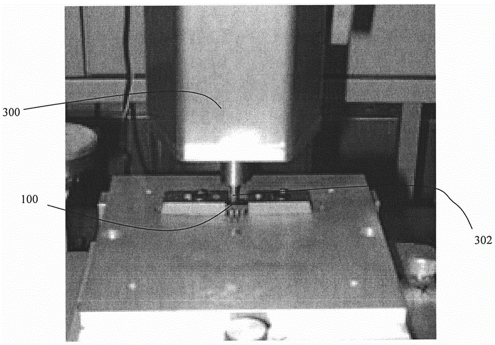
[0031] see figure 1 and figure 2 The semiconductor device 100 of the present invention has a main body 101 and three pins 106 extending from one side of the main body 101 . The main body 101 has a front (not numbered) and an opposite back 102 . The backside 102 has a copper layer, a silicon layer 104 and a chip stack 108 in sequence. The failure analysis method of the semiconductor device 100 of the present invention comprises the following steps:

[0032] S101 : removing the copper layer on the back surface 102 of the semiconductor device 100 .

[0033] The present invention uses 70% nitric acid solution 200 to etch away the copper layer on the back surface 102 of the main body 101 of the semiconductor device 100 . In order to prevent the pins 106 from being corroded by the nitric acid solution 200, the three pins 106 need to be well protected. In order to reduce the cost, in this step, the method of controlling the liquid level of the nitric acid solution 200 is adopte...


PUM


Abstract

The present invention relates to a failure analysis method of a semiconductor device, which comprises the steps of: removing the copper layer on the back of the semiconductor device; thinning the silicon layer on the back of the semiconductor device; and using a low-light microscope (Emission Microscope, EMMI) and / or laser Optical Beam Induced Impedance Change (OBIRCH) electrical location equipment locates failure points on the backside of semiconductor devices. The failure analysis method of the semiconductor device of the present invention saves time and improves efficiency and success rate by removing copper, thinning the silicon layer and locating the failure point on the back of the semiconductor device.

Description

technical field [0001] The invention relates to the technical field of semiconductor testing, in particular to a failure analysis method for semiconductor devices. Background technique [0002] For the mass production of semiconductor devices, it is desirable to provide a profitable and reliable process technology. A process for improving reliability and stability of process technology includes the steps of designing a semiconductor device, manufacturing a sample of the semiconductor device, and testing the sample. Failure analysis of semiconductor devices is a feedback process designed to discover and correct the root cause of defects to overcome the problems created by the defects. [0003] Proper failure analysis is critical to improving the quality of semiconductor devices. Incorrect failure analysis can lengthen the period required to develop and ramp up semiconductor device products. Generally, failure analysis includes external inspection, non-destructive analysis,...

Claims


Application Information

Patent Timeline
Patent Type & Authority Patents(China)
IPC IPC(8): G01R31/307G01R31/308
Inventor 韦俊董红
Owner CSMC TECH FAB2 CO LTD
Features
  • R&D
  • Intellectual Property
  • Life Sciences
  • Materials
  • Tech Scout
  • Unparalleled Data Quality
  • Higher Quality Content
  • 60% Fewer Hallucinations
Learn More