Sub-wavelength dielectric-loaded surface plasma optical waveguide

A medium-loaded, surface plasmon technology, which is applied in the field of optical waveguides, can solve the problems of poor confinement ability and large mode field area of ​​plasmon optical waveguide field, and achieve reduced transmission loss, enhanced field enhancement effect, and horizontal and vertical dimensions. zoom out effect

Inactive Publication Date: 2012-07-11
BEIHANG UNIV
View PDF3 Cites 3 Cited by
  • Summary
  • Abstract
  • Description
  • Claims
  • Application Information

AI Technical Summary

Problems solved by technology

[0006] The purpose of the present invention is to overcome the defects of large mode field area and poor confinement ability of the medium-loaded surface plasmon optical waveguide based on low refractive index materials, and propose a medium with subwavelength mode field confinement capability and lower transmission loss Loaded Surface Plasmon Optical Waveguide Structure

Method used


Image

  • Sub-wavelength dielectric-loaded surface plasma optical waveguide
  • Sub-wavelength dielectric-loaded surface plasma optical waveguide
  • Sub-wavelength dielectric-loaded surface plasma optical waveguide

Examples


example

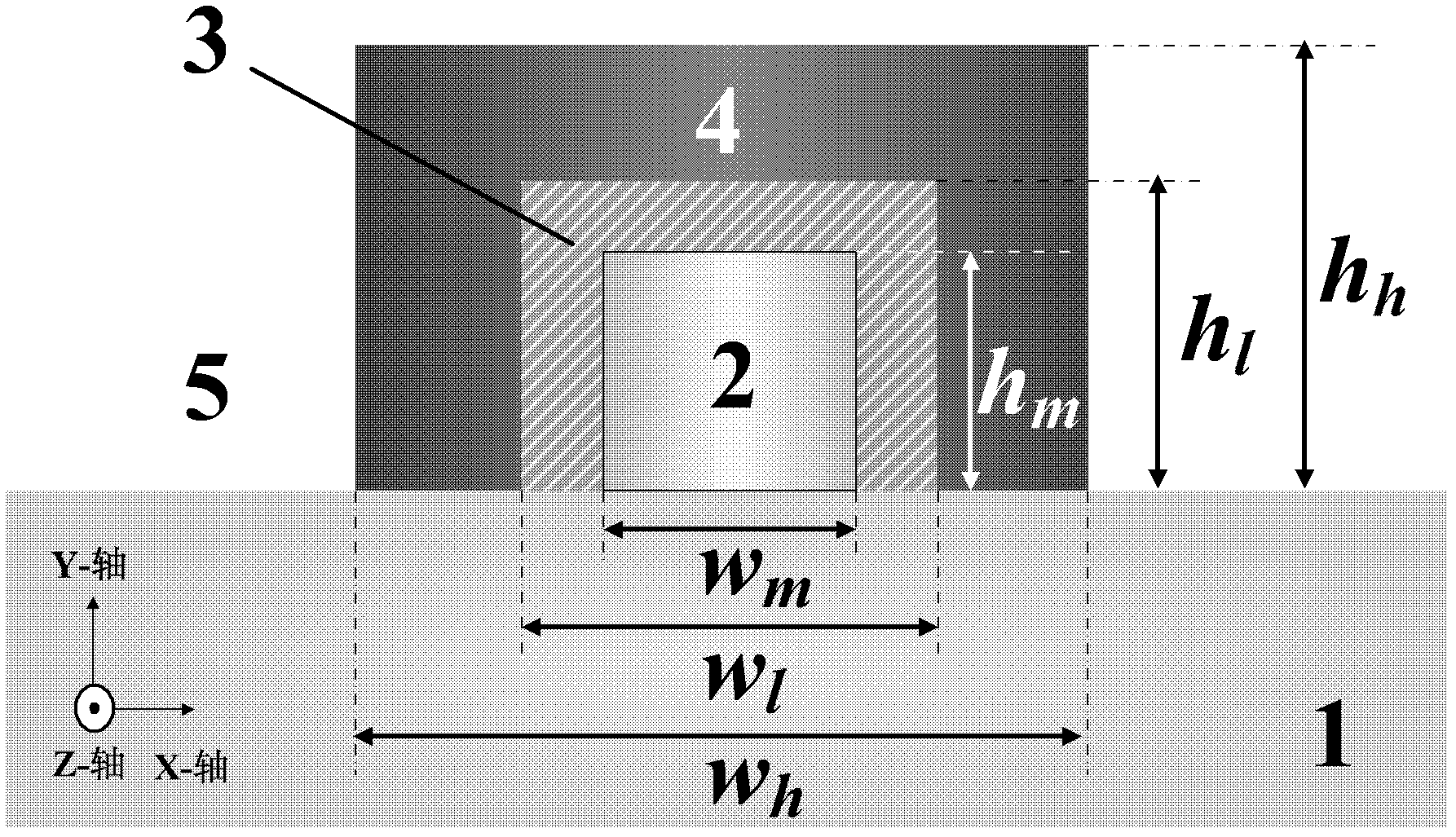
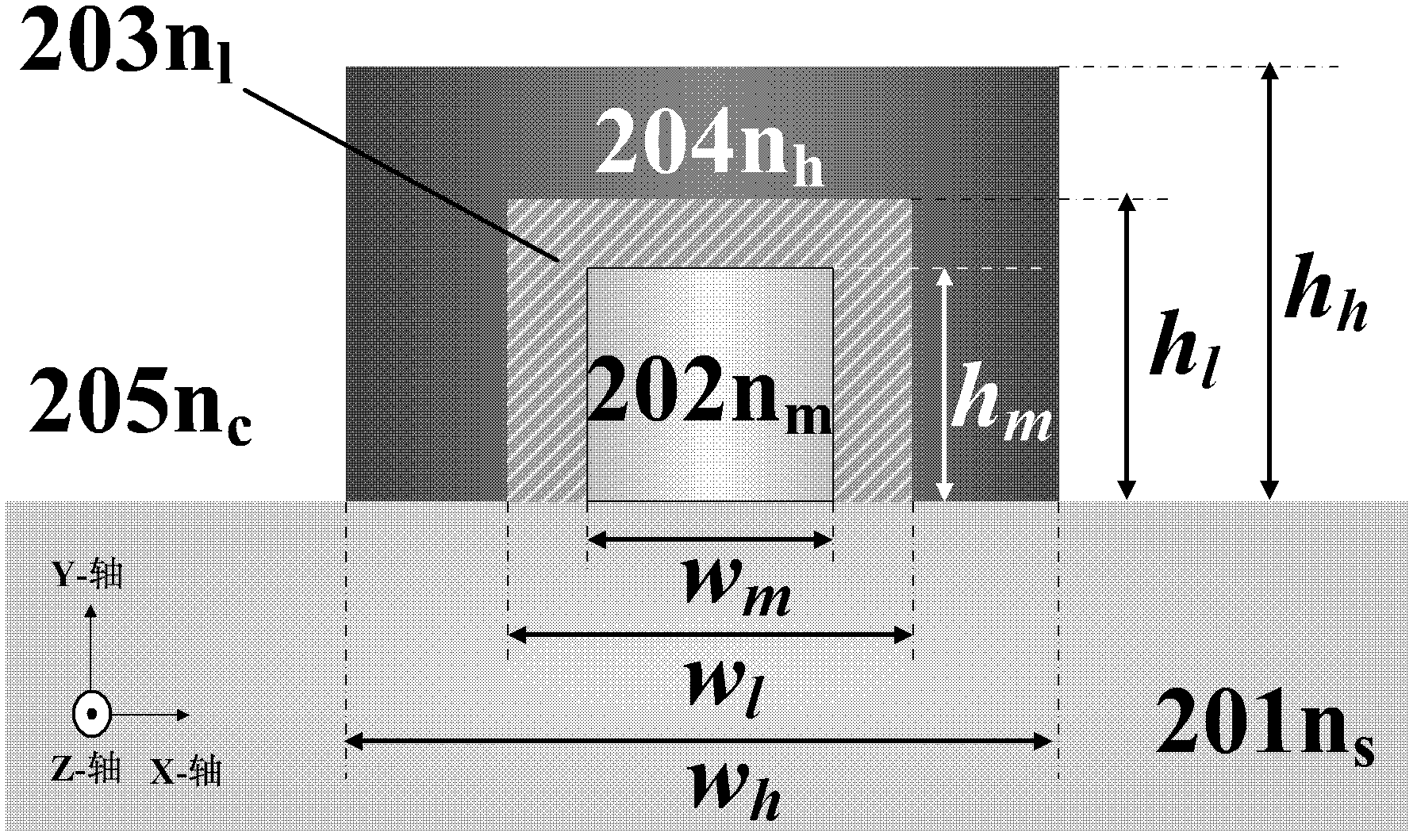
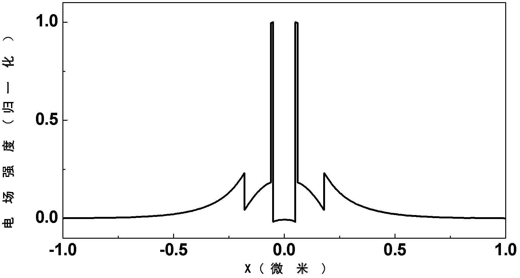
[0036] figure 2 It is the structural diagram of the dielectric-loaded surface plasmon optical waveguide described in the example. 201 is the dielectric base layer, n s Its refractive index; 202 is the metal nanorod, n m is its refractive index, its cross-section is square, and its width is w m , with height h m ; 203 is the low refractive index medium area, n l is its refractive index, w l its width, h l Its height; 204 is the high emissivity medium area, n h is its refractive index, w h its width, h h Its height; 205 is the cladding, n c for its refractive index.

[0037] In this example, the wavelength of the transmitted optical signal is selected as 1.55 μm, the material of 201 and 203 is set as silicon dioxide, and its refractive index is 1.5; the material of 202 is silver, and its refractive index at 1.55 μm wavelength is 0.1453 +i*11.3587; the material of 204 is silicon, and its refractive index is 3.5; the material of 205 is air, and its refractive index is ...


PUM


Abstract

The invention discloses a dielectric-loaded surface plasma optical waveguide with a sub-wavelength optical field limit capacity. The cross section of the waveguide structure comprises a dielectric basement layer (1), a metal area (2), a low-refractive-index dielectric area (3), a high-refractive-index dielectric area (4) and a cladding (5), wherein the metal area (2) is positioned on the basementlayer, the low-refractive-index dielectric area (3) is used for cladding the metal area, and the high-refractive-index dielectric area is used for cladding the metal area and the low-refractive-indexdielectric area. As the high-refractive-index dielectric area exists, the distribution range of optical fields of the waveguide structure can be significantly shrunk, and the two-dimension sub-wavelength restriction for transmission optical fields is realized. Meanwhile, as the low-refractive-index dielectric area exists, the waveguide still can keep lower transmission loss. The optical waveguidegreatly realizes the balance between the optical field limit capacity and the transmission loss and provides probability for the realization of an optical waveguide chip with an ultrahigh integrated level.

Description

technical field [0001] The invention relates to the field of optical waveguide technology, in particular to a subwavelength medium-loaded surface plasmon optical waveguide. Background technique [0002] In recent years, surface plasmon photonics technology has shown great application potential in the field of nanophotonics due to its unique advantages. A surface plasmon is a pattern of electromagnetic waves caused by the interaction of light and free electrons on the surface of a metal. This mode exists near the metal-dielectric interface, and its field strength reaches its maximum at the interface, and decays exponentially on both sides of the interface along the direction perpendicular to the interface. Surface plasmons have strong field confinement properties, which can confine the field energy to a region whose spatial size is much smaller than its free-space transmission wavelength, and its properties can change with the change of the metal surface structure. In the s...

Claims


Application Information

Patent Timeline
Patent Type & Authority Applications(China)
IPC IPC(8): G02B6/10
Inventor 郑铮卞宇生赵欣苏亚林刘磊刘建胜
Owner BEIHANG UNIV
Why Eureka
Try Eureka