Array substrate and liquid crystal display

A liquid crystal display and array substrate technology, applied in the field of liquid crystal display, can solve problems such as display differences in corner areas, and achieve the effects of reducing display differences, improving display image quality, and improving aperture ratio and display contrast.

Active Publication Date: 2012-07-11
BOE TECH GRP CO LTD +1
View PDF4 Cites 18 Cited by
  • Summary
  • Abstract
  • Description
  • Claims
  • Application Information

AI Technical Summary

Problems solved by technology

[0007] The present invention provides an array substrate and a liquid crystal display, which solves the problem of display differences in corner regions of pixel units on an array substrate in the prior art, so as to reduce display differences in corner regions of pixel units and improve aperture ratio and display contrast

Method used


Image

  • Array substrate and liquid crystal display
  • Array substrate and liquid crystal display
  • Array substrate and liquid crystal display

Examples


Embodiment 1

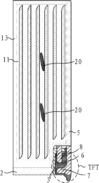
[0029] Figure 2A A schematic diagram of a partial top view structure of the array substrate provided in Embodiment 1 of the present invention, as shown in Figure 2A As shown, the array substrate includes a base substrate (not shown in the figure), and the pixel area of ​​the base substrate is formed with data lines 5 and gate lines 2 that cross horizontally and vertically to form a plurality of pixel units, and each pixel The unit 30 includes a switching element TFT, a pixel electrode 11 and a common electrode 13, and the common electrode 13 in each pixel unit 30 has a slit 131, wherein:

[0030] The slits 131 of the common electrode 13 and / or the pixel electrode in each pixel unit 30 are zigzag-shaped, and the slits are parallel to each other, forming a slit area, Figure 2A In the above, the common electrode is above the pixel electrode, and the shape of the slit of the common electrode is zigzag as an example. If the common electrode is below the pixel electrode, the sha...

Embodiment 2

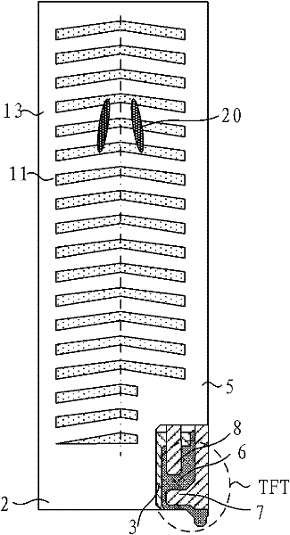
[0036] image 3 A schematic diagram of a partial top view structure of the array substrate provided in Embodiment 2 of the present invention, as shown in image 3 As shown, the array substrate includes a base substrate, the pixel area of ​​the base substrate is formed with data lines 5 and gate lines 2 that cross horizontally and vertically to form a plurality of pixel units 30, and each pixel unit 30 includes a switch The element TFT, the pixel electrode 11 and the common electrode 13, the common electrode 13 in each pixel unit 30 has a slit 131, wherein: the shape of the slit 131 of the common electrode 13 in each pixel unit 30 is a zigzag shape, and each slit 131 are parallel to each other to form a slit area; the edge of the pixel electrode 11 pattern is parallel to the edge of the slit area; the gate line 2 and / or data line 5 is parallel to the edge of the adjacent pixel electrode pattern.

[0037] Further, the bending directions of the patterns of the pixel electrodes 1...

Embodiment 3

[0047] Figure 4 A schematic diagram of a partial top view structure of the array substrate provided in Embodiment 3 of the present invention, as shown in Figure 4 As shown, the array substrate includes a base substrate, the pixel area of ​​the base substrate is formed with data lines 5 and gate lines 2 that cross horizontally and vertically to form a plurality of pixel units 30, and each pixel unit 30 includes a switch The element TFT, the pixel electrode 11 and the common electrode 13, the common electrode 13 in each pixel unit 30 has a slit 131, wherein: the shape of the slit 131 of the common electrode 13 in each pixel unit 30 is a zigzag shape, and each slit 131 are parallel to each other to form a slit area; the edge of the pixel electrode 11 pattern is parallel to the edge of the slit area; the gate line 2 and / or data line 5 is parallel to the edge of the adjacent pixel electrode pattern.

[0048] Further, the pixel units 30 are arranged in a matrix.

[0049] In addi...


PUM

PropertyMeasurementUnit
widthaaaaaaaaaa

Abstract

The invention discloses an array substrate and a liquid crystal display. The array substrate comprises a lining substrate, data lines and grid lines are transversely and longitudinally intersected to form a plurality of pixel units and formed in a pixel area of the lining substrate, each pixel unit comprises a switch element, a pixel electrode and a public electrode, and the public electrode of each pixel unit is provided with a slit. The slit of the public electrode and / or pixel electrode of each pixel unit is in a shape of a fold line, the slits are mutually parallel to form a slit area, and the edge of a pixel electrode pattern is parallel to the edge of the slit area. The slit of the public electrode of each pixel unit is in the shape of the fold line, the edge of the pixel electrode pattern is parallel to the edge of the slit area, and each integral pixel unit is accordant to bending of a corresponding electric field in shape, so that the electric field in each pixel unit is uniform in distribution, displaying uniformity of the pixel units is improved, and aperture ratio and displaying contrast ratio are increased.

Description

technical field [0001] The invention relates to liquid crystal display technology, in particular to an array substrate and a liquid crystal display. Background technique [0002] A liquid crystal display is a commonly used flat panel display at present, and a Thin Film Transistor Liquid Crystal Display (TFT-LCD for short) is a mainstream product in the liquid crystal display. [0003] LCD can be divided into various types according to different forms of electric field, including Advanced-Super Dimensional Switching (AD-SDS), which generates parallel electric fields and The vertical electric field generated between the pixel electrode layer and the common electrode layer forms a multi-dimensional spatial compound electric field, which enables rotation conversion of all oriented liquid crystal molecules between the pixel electrodes and directly above the electrodes in the liquid crystal cell, thereby improving the working efficiency of the planar oriented liquid crystal and in...

Claims


Application Information

Patent Timeline
Patent Type & Authority Applications(China)
IPC IPC(8): G02F1/1343G02F1/1362G02F1/1368G02F1/1337H01L27/02
CPCG02F1/134309G02F2001/134318G02F1/134363G02F2201/52G02F1/134318
Inventor 杨瑞智林准焕黄炜赟
Owner BOE TECH GRP CO LTD
Why Eureka
Try Eureka