

Double-gate TFT (thin film transistor) substrate and production method thereof
A manufacturing method and substrate technology, applied in semiconductor/solid-state device manufacturing, optics, instruments, etc., can solve the problems of wasting IC joints and reducing pixel aperture ratio, and achieve the effect of saving costs and preventing green defects
- Summary
- Abstract
- Description
- Claims
- Application Information
AI Technical Summary
Problems solved by technology
Method used
Image

Examples
Embodiment Construction
[0020] The following will clearly and completely describe the technical solutions in the embodiments of the present invention with reference to the accompanying drawings in the embodiments of the present invention. Obviously, the described embodiments are only some, not all, embodiments of the present invention. Based on the embodiments of the present invention, all other embodiments obtained by persons of ordinary skill in the art without making creative efforts belong to the protection scope of the present invention.
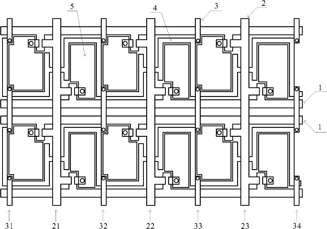
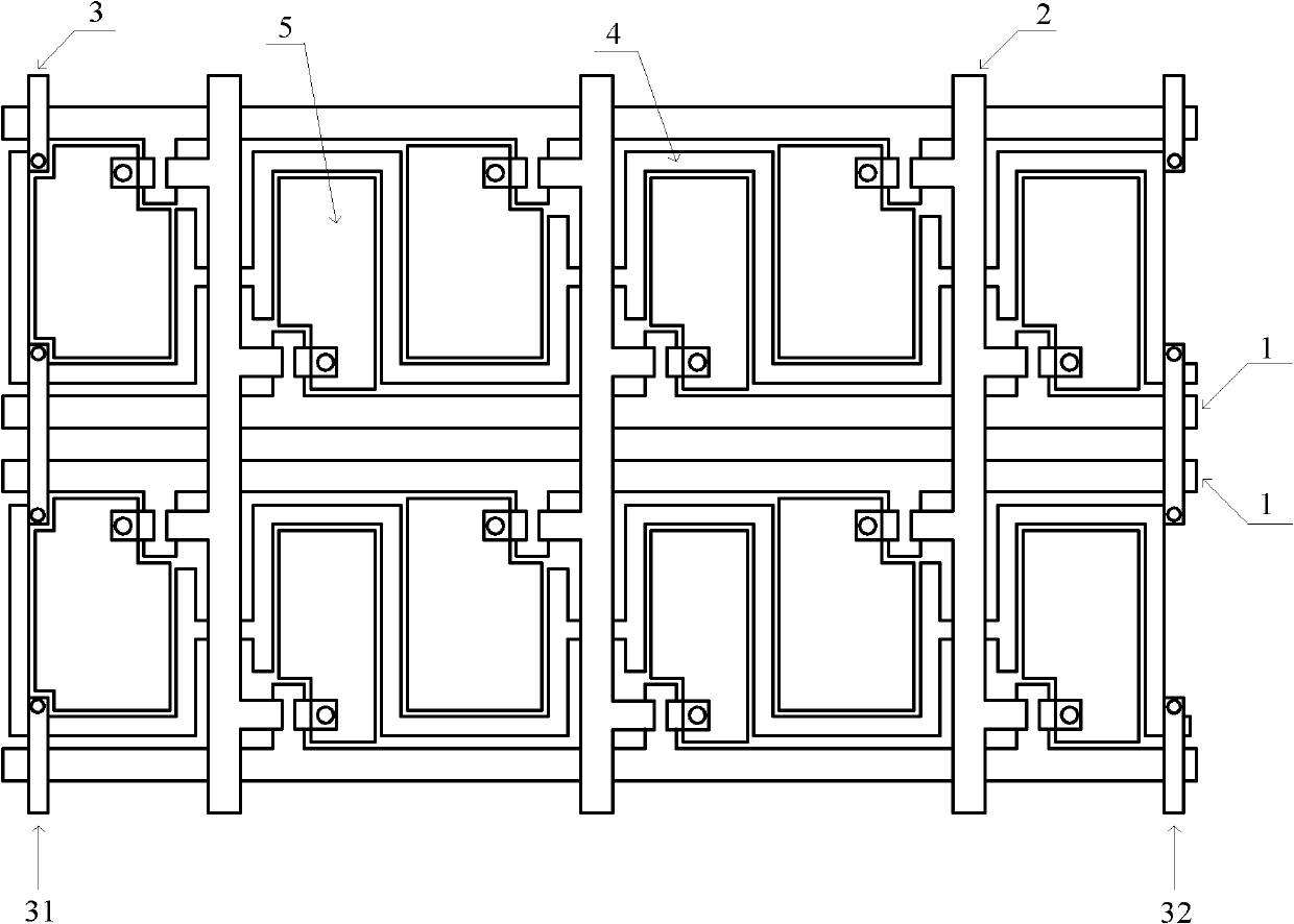
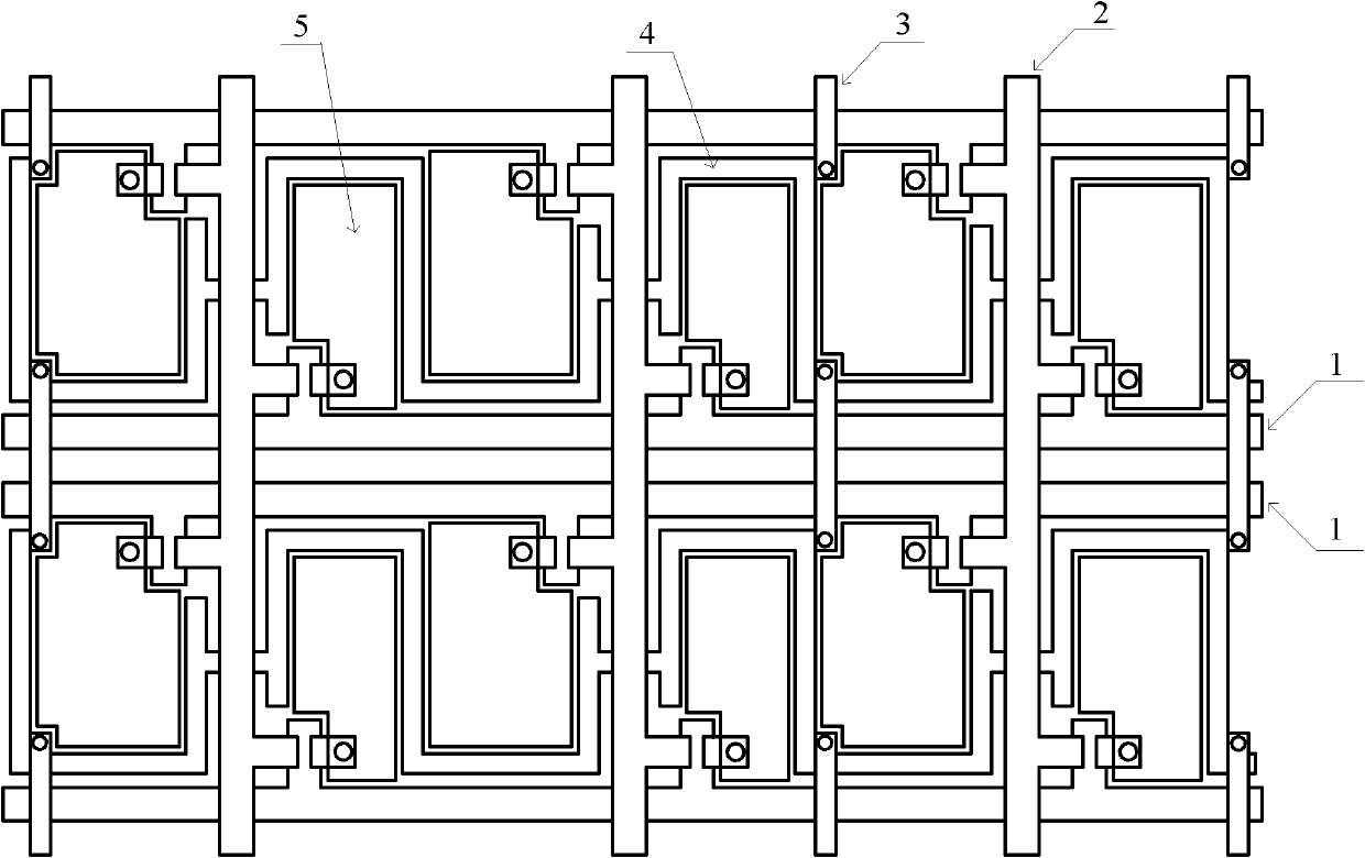
[0021] The double-gate TFT substrate provided by the embodiment of the present invention, such as figure 2 shown, including:
[0022] A glass substrate (not shown in the figure), a horizontal gate line 1 , a mesh Vcom line 4 , a vertical data line 2 , and a pixel unit 5 defined by intersections of the horizontal gate line 1 and the vertical data line 2 . Wherein, each Vcom line of each row of the mesh Vcom line 4 is electrically connected respectively, and t...
PUM
 Abstract
Description
Claims
Application Information