Non-destructive welding device of micro-PCB (printed circuit board) device

A welding device and miniature technology, which is applied in the direction of assembling printed circuits with electric components, can solve the problem of inability to realize the repair welding of micro-PCB components that are not resistant to high temperature, and achieve the requirements of improving operation efficiency and process implementation accuracy and reducing operation skills , Solve the effect of manual patching or dismantling

Inactive Publication Date: 2012-07-11
SHENYANG CHENXUN SIMCOM TECH
View PDF0 Cites 3 Cited by
  • Summary
  • Abstract
  • Description
  • Claims
  • Application Information

AI Technical Summary

Problems solved by technology

[0004] The technical problem to be solved by the present invention is to overcome the defect that soldering tools such as electric soldering irons in the prior art cannot realize the repair welding of micro-PCB parts that ar

Method used


Image

  • Non-destructive welding device of micro-PCB (printed circuit board) device
  • Non-destructive welding device of micro-PCB (printed circuit board) device
  • Non-destructive welding device of micro-PCB (printed circuit board) device

Examples


Embodiment Construction

[0032] The preferred embodiments of the present invention are given below in conjunction with the accompanying drawings to describe the technical solution of the present invention in detail.

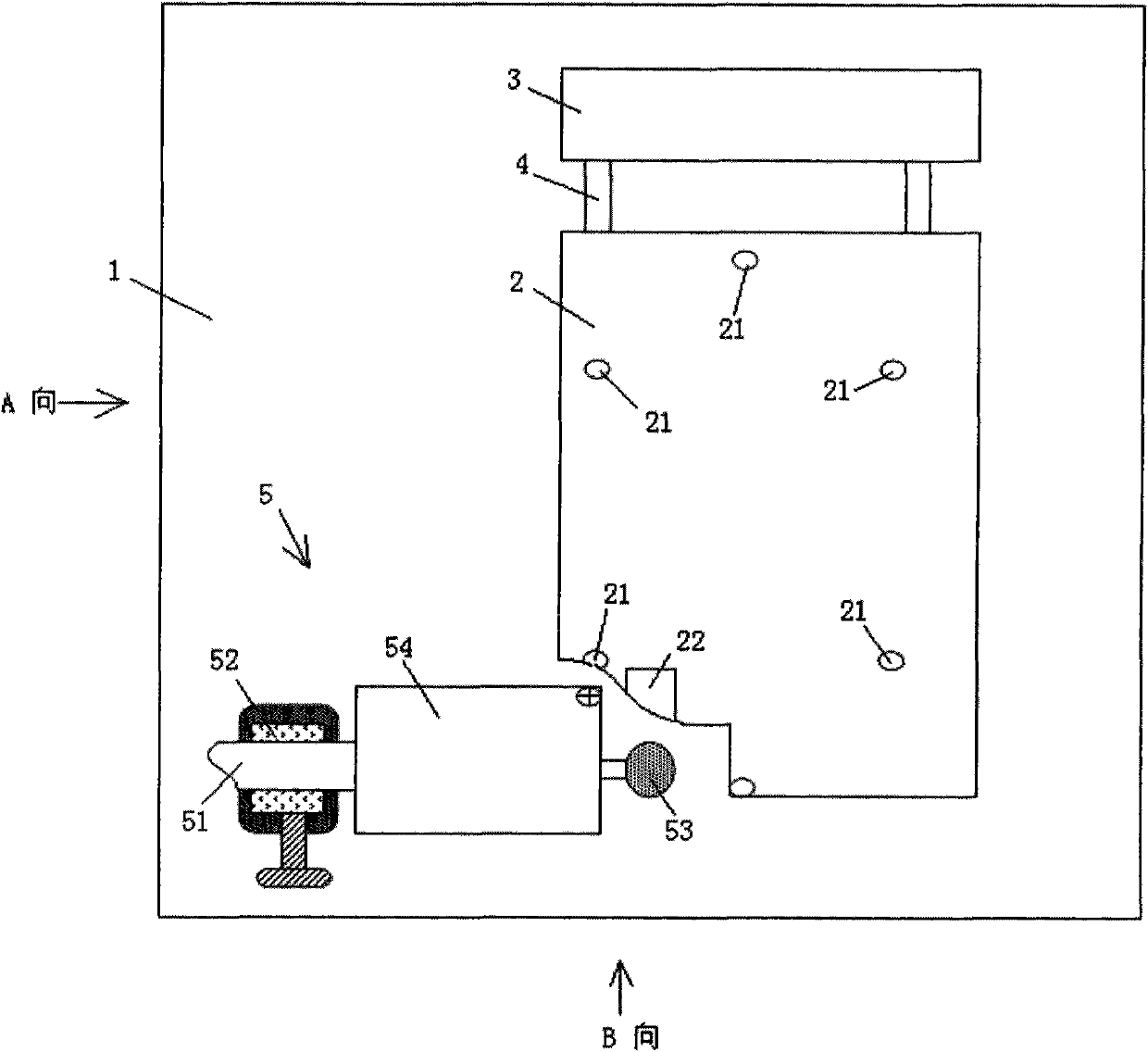
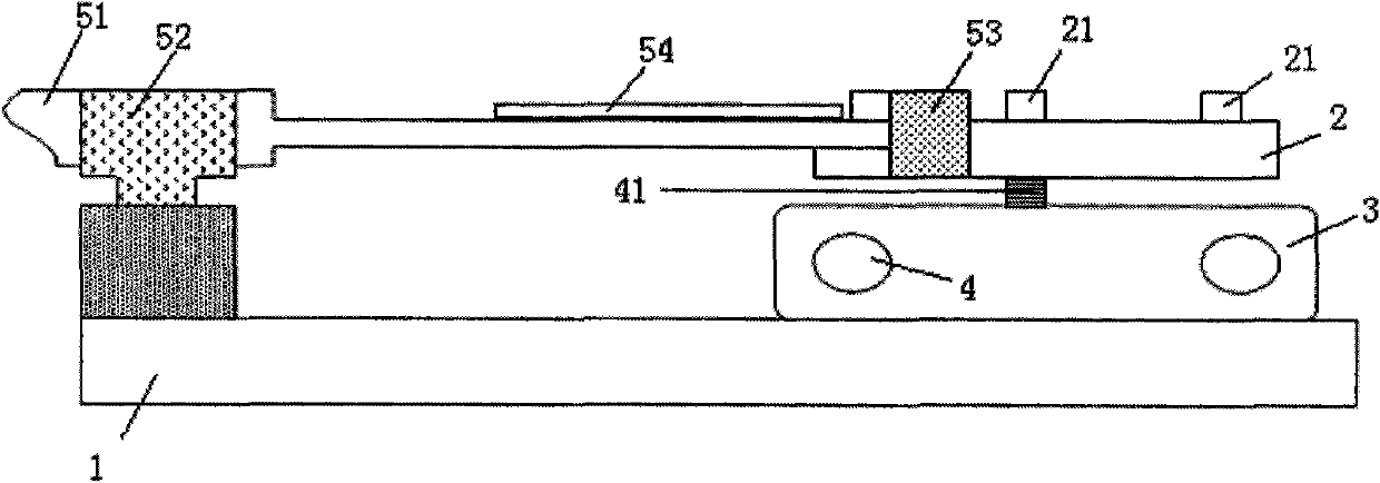
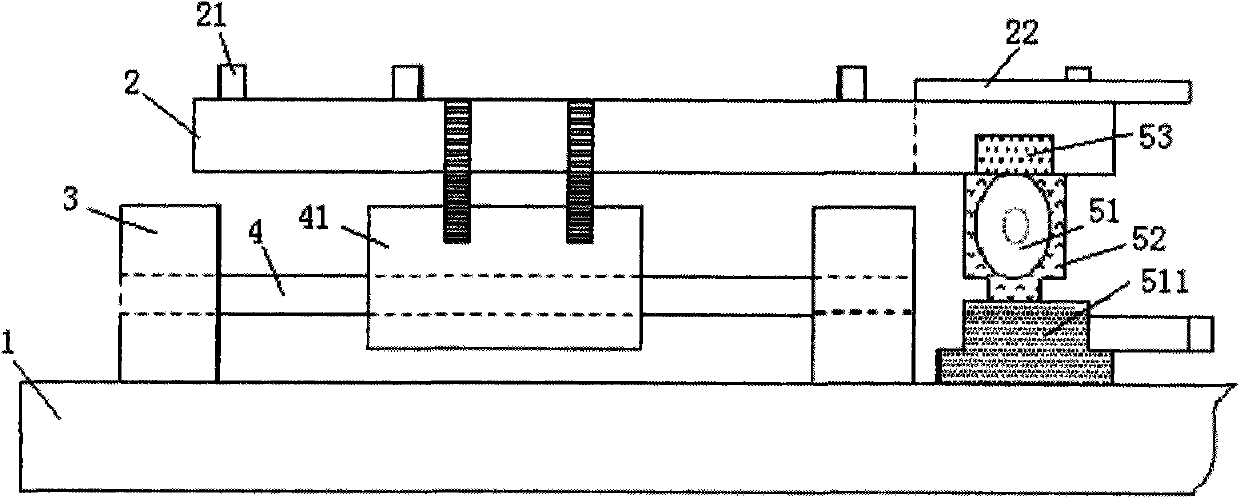
[0033] Such as Figure 1 to Figure 3 As shown, the present invention provides a kind of non-destructive soldering tool for partial parts of micro PCB, comprising a bottom plate 1, one movable on the bottom plate 1, and a transfer platform 2 for placing and moving the micro PCB; one fixed on one side of the bottom plate 1 The heating device 5. The heating device 5 is close to one side of the transfer platform 2 and is located below the plane where the transfer platform 2 is located. In this way, when the micro PCB moves above the heating device 5, the bottom of the micro PCB can be heated by the heating device 5, so as to complete the non-destructive welding of the local components of the micro PCB.

[0034] Preferably, the heating device 5 of the present invention may include: a heater...


PUM

PropertyMeasurementUnit
Thicknessaaaaaaaaaa

Abstract

The invention discloses a non-destructive welding device of a micro-PCB (printed circuit board) device. The non-destructive welding device comprises a bottom board, a moving platform which is movably arranged on the bottom board and further used for moving a micro-PCB and a heating device which is fixedly arranged on the bottom board, wherein the heating device is close to one side of the moving platform. The non-destructive welding device disclosed by the invention can solve the follow-up industry process that a device without the resistance to high temperature can not be repair-welded in a device dense region by an electric iron agent, a hot air gun and the like of the PCB, effectively solve the feasibility of a PCB local welding process, reduce the requirements on operation skills of operators and improve operation efficiency and process implementation precision in a breakthrough manner.

Description

technical field [0001] The invention relates to a welding device, in particular to a non-destructive welding device for micro PCB devices. Background technique [0002] At present, in the SMT industry, subsequent repair welding or adjustment of some devices on the micro PCB (micro PCB refers to a single / double-sided printed circuit board with a thickness of no more than 1 mm) is usually required. The repair soldering of existing local devices usually adopts electric soldering iron or hot air heater, that is, manually holds such tools to carry out soldering or disassembly of devices. However, in this process, operators need to have high professional skills and experience. In addition, such tools work inefficiently and weld quality is often not guaranteed. [0003] With the miniaturization of the components to be soldered and the high density of the components of the micro PCB, the soldering method of the electric soldering iron has been unable to function. Moreover, many p...

Claims


Application Information

Patent Timeline
IPC IPC(8): H05K3/34
Inventor 刘家仁
Owner SHENYANG CHENXUN SIMCOM TECH
Why Eureka
Try Eureka