Method for reducing grounding resistance and thermal resistance of printed board

A grounding resistance and printed board technology, applied in the direction of assembling printed circuits with electrical components, can solve the problems of large grounding resistance and thermal resistance of printed boards, reduce grounding resistance and thermal resistance, and ensure technical indicators and reliability. sexual effect

Inactive Publication Date: 2012-07-11
SICHUAN LONGRUI MICROELECTRONICS
View PDF4 Cites 1 Cited by
  • Summary
  • Abstract
  • Description
  • Claims
  • Application Information

AI Technical Summary

Problems solved by technology

[0004] In order to overcome the problem of large grounding resistance and thermal resistance of the printed board in the existing assembly method, the present invention provides a method for reducing the grounding resistance and thermal resistance of the printed board to ensure the technical indicators and reliability of the transmitter

Method used


Image

  • Method for reducing grounding resistance and thermal resistance of printed board
  • Method for reducing grounding resistance and thermal resistance of printed board
  • Method for reducing grounding resistance and thermal resistance of printed board

Examples


Embodiment Construction

[0013] The present invention is further explained below in conjunction with the examples, but the examples do not limit the present invention in any form.

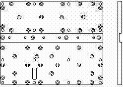
[0014] (1) Prepare the copper carrier plate and clean it with alcohol cotton balls, see figure 1 .

[0015] (2) Fasten the carrier board to the cavity with screws.

[0016] (3) Clean the printed board with alcohol cotton ball.

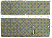
[0017] (4) Apply a layer of solder paste evenly on the printed board through the screen, see figure 2 .

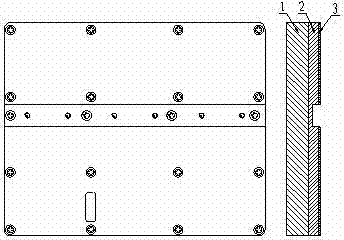
[0018] (5) Fasten the printed board coated with solder paste on the carrier board with screws, see image 3 .

[0019] (6) Clean the outflowing solder paste with alcohol cotton ball.

[0020] (7) Bake the fastened cavity, carrier board and printed board in a high-temperature oven at a temperature of 240°C for 5 minutes. It is necessary to ensure that the printed board does not have blisters, the metal color difference does not change much, and there is no obvious gap between the printed...


PUM


Abstract

The invention discloses a method for reducing grounding resistance and thermal resistance of a printed board, belonging to the field of electronics assembly technology in an electronic information industry; the method comprises the steps of manufacturing a red copper substrate of which the area is more than that of the circuit printed board, using an alcohol cotton ball to clean the circuit printed board; using the alcohol cotton ball to clean the circuit printed board; uniformly coating solder paste on the back of the cleaned printed board by a silk screen; fixing the printed board coated with solder paste and the red copper substrate together on a cavity by a screw under conditions that the fixation is not too tight and is justly proper, and small amount of the solder paste flows out; using the alcohol cotton ball to clean the outflowed solder paste; putting the fastened chamber, the substrate and the printed board to a high-temperature box to bake for 5 min at 240 DEG C; after baking, taking out to cool, and then using the alcohol cotton ball to clean; welding a high-power transistor and other component on the printed board and the substrate. The method has the advantage that the grounding resistance and the thermal resistance of the printed board can be reduced and the technical index and the reliability of a transmitter are ensured.

Description

technical field [0001] The invention belongs to the technical field of electronic assembly in the electronic information industry. It relates to a method for reducing grounding resistance and thermal resistance of printed boards. Background technique [0002] A large number of high-power transistors and their circuit printed boards are used in transmitters of electronic equipment such as radar, navigation, and communication, so higher requirements are placed on the reliability of printed boards, and the grounding resistance and thermal resistance of printed boards are the most important factors. Two important factors of reliability. [0003] At present, in the transmitter, the high-power transistor and its circuit printed board are fixed on the cavity by screws. However, due to the unevenness of the printed board, the grounding resistance and thermal resistance between the printed board and the cavity are large, resulting in self-excitation of the circuit, poor thermal con...

Claims


Application Information

Patent Timeline
IPC IPC(8): H05K3/34
Inventor 弋建利熊正花赵治军刘军赵庆香罗俊杰
Owner SICHUAN LONGRUI MICROELECTRONICS
Why Eureka
Try Eureka