Method for recovering pattern sapphire substrate

A patterned sapphire and substrate technology, which is applied in the field of optoelectronics, can solve the problems that PSS cannot be reused and the production cost is high, and achieve the effects of short recycling cycle, improved utilization rate and simple recycling method

Active Publication Date: 2012-07-18
HC SEMITEK CORP
View PDF5 Cites 24 Cited by
  • Summary
  • Abstract
  • Description
  • Claims
  • Application Information

AI Technical Summary

Problems solved by technology

[0005] In order to solve the problems in the prior art that PSS cannot be reused and the production cost is high, the embodiment of the present invention provides a method for recovering PSS

Method used


Image

  • Method for recovering pattern sapphire substrate
  • Method for recovering pattern sapphire substrate
  • Method for recovering pattern sapphire substrate

Examples


Embodiment 1

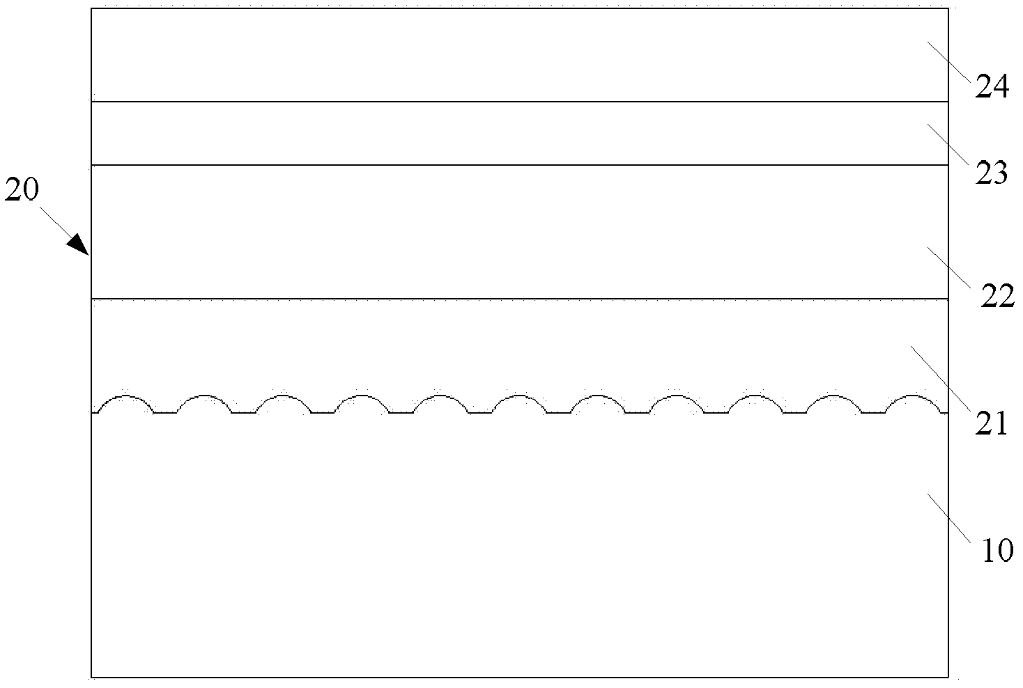
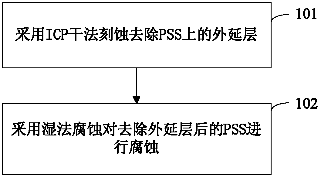
[0024] Such as figure 2 As shown, the embodiment of the present invention provides a kind of method of reclaiming PSS, and this method comprises:

[0025] Step 101: using ICP dry etching to remove the epitaxial layer on the PSS.

[0026] Dry etching is used to ensure that the epitaxial layer is completely etched, and the damage to the substrate material is small.

[0027] Step 102: Etching the PSS after removing the epitaxial layer by wet etching.

[0028] After wet etching, defects such as etching damage and dirt caused by dry etching on the PSS are removed, and a reusable PSS is obtained.

[0029] In the embodiment of the present invention, the epitaxial layer on the PSS is removed by ICP dry etching, and then the etching damage and dirt caused by dry etching are removed by wet etching, so as to obtain a reusable PSS, which greatly improves the The utilization rate of PSS is improved, thereby reducing the production cost of LED. In addition, the recycling method is simp...

Embodiment 2

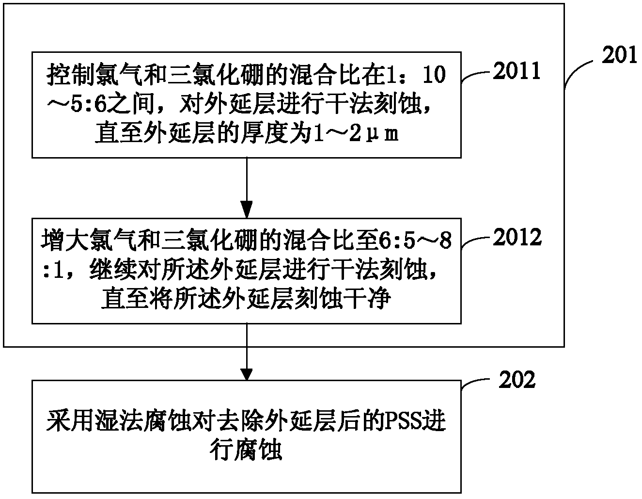
[0031] In this embodiment, taking , as an example, the embodiment of the present invention is described in detail. Such as image 3 As shown, the present embodiment provides a method for reclaiming a patterned sapphire substrate, the method comprising:

[0032] Step 201: using ICP dry etching to remove the epitaxial layer on the PSS.

[0033] Specifically, a mixed gas of chlorine gas and boron trichloride is used as the main reaction gas for ICP dry etching.

[0034] The mixed gas of chlorine gas and boron trichloride is used as the main reaction gas, which can effectively remove the epitaxial layer on the PSS without damaging the PSS material and avoiding damage to the patterned appearance of the PSS.

[0035] Preferably, this step specifically includes:

[0036] Step 2011: Control the mixing ratio of chlorine gas and boron trichloride between 1:10-5:6, and perform dry etching on the epitaxial layer until the thickness of the epitaxial layer is 1-2 μm.

[0037] Controllin...


PUM

PropertyMeasurementUnit
thicknessaaaaaaaaaa

Abstract

The embodiment of the invention discloses a method for recovering a pattern sapphire substrate (PSS). The method belongs to the field of photovoltaic technology. The method comprises the following steps: removing an epitaxial layer on the pattern sapphire substrate by adopting an inductively coupled plasma (ICP) dry etching method; and etching the pattern sapphire substrate by adopting a wet etching method after the epitaxial layer is removed. In the embodiment of the method, the epitaxial layer on the PSS is removed by the ICP dry etching method and then the defects of etching damage, squalidity, and the like caused by the dry etching are removed by the wet etching, so that the PSS which can be reused is obtained, the utilization ratio of the PSS is greatly improved, and the production cost of the LED (light-emitting diode) is reduced.

Description

technical field [0001] The invention relates to the field of optoelectronic technology, in particular to a method for recycling a patterned sapphire substrate. Background technique [0002] In the manufacturing process of LED (Light Emitting Diode, light-emitting diode) and other optoelectronic devices, sapphire substrates are widely used, which are usually divided into flat sapphire substrates and PSS (Pattern Sapphire Substrate, patterned sapphire substrates). Among them, PSS is made on a flat sapphire substrate by processing a pattern array with a certain shape and a size on the order of micronano. Therefore, PSS is more and more widely used in the growth process of LED epitaxial wafers. [0003] During the growth of LED epitaxial wafers and the later processing of LED chips, scrapped sheets are often produced. In order to reduce production costs, it is necessary to remove the epitaxial layer of these scrapped sheets and recycle the sapphire substrate for reuse. The exi...

Claims


Application Information

Patent Timeline
Patent Type & Authority Applications(China)
IPC IPC(8): H01L33/00
Inventor 张建宝刘秋艳刘榕兰叶周武
Owner HC SEMITEK CORP
Why Eureka
Try Eureka