Pixel circuit and display apparatus
一种像素电路、显示装置的技术,应用在静态指示器、仪器等方向,能够解决平均电位降低、无法获得对比度等显示质量等问题
- Summary
- Abstract
- Description
- Claims
- Application Information
AI Technical Summary
Problems solved by technology
Method used
Image

Examples
no. 1 approach
[0129] In the first embodiment, configurations of a display device of the present invention (hereinafter simply referred to as "display device") and a pixel circuit of the present invention (hereinafter simply referred to as "pixel circuit") will be described.
[0130] 【Display device】
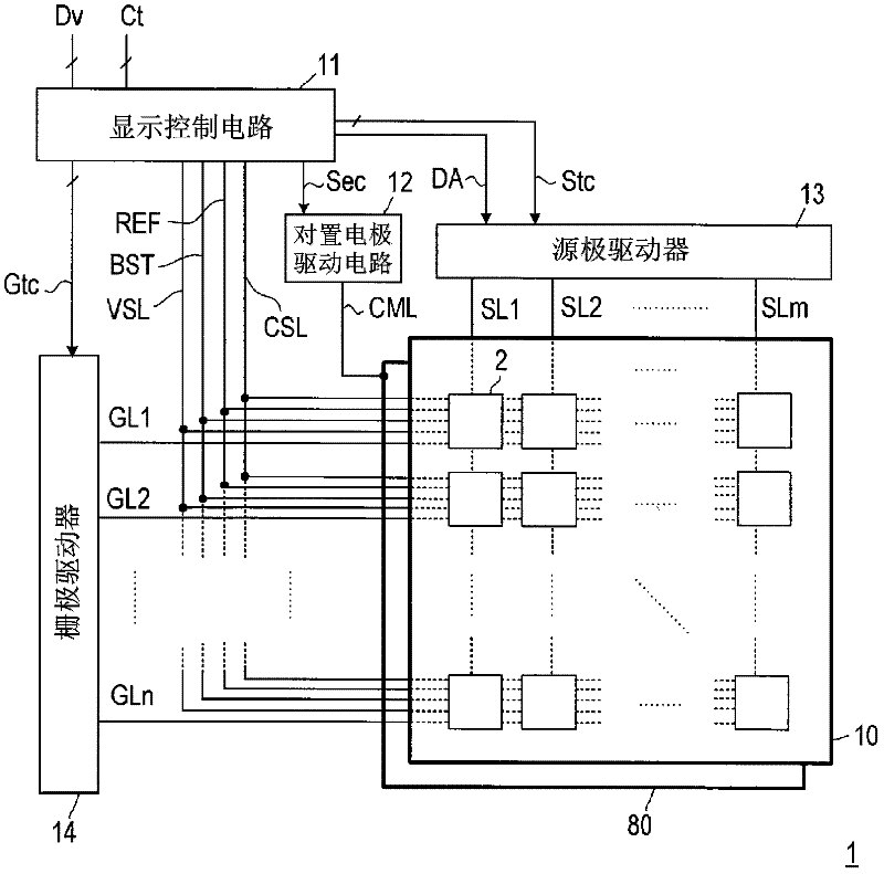
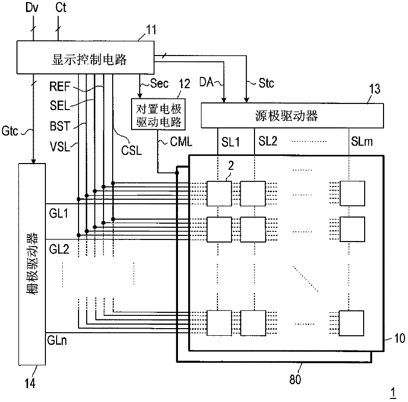
[0131] figure 1 A schematic configuration of the display device 1 is shown. The display device 1 includes an active matrix substrate 10 , opposing electrodes 80 , a display control circuit 11 , an opposing electrode driving circuit 12 , a source driver 13 , a gate driver 14 , and various signal lines described later. On the active matrix substrate 10, a plurality of pixel circuits 2 are respectively arranged in the row and column directions, forming a pixel circuit array.
[0132] In addition, in figure 1 In , in order to avoid complicated drawings, the pixel circuit 2 is shown in blocks. In addition, in order to clearly show that various signal lines are formed on the active matrix subs...
no. 2 approach
[0191] In the second embodiment, the self-refresh operation of each of the first to third types of pixel circuits described above will be described with reference to the drawings.
[0192] The self-refresh operation refers to operating the first switch circuit 22, the second switch circuit 23, and the control circuit 24 at a predetermined timing for a plurality of pixel circuits 2 in the operation of the continuous display mode, and making the pixel circuits 20 The operation of returning the potential (also the potential of the internal node N1) to the potential of the gray level written in the previous write operation is aimed at the pixel circuits of all gray levels, simultaneously and uniformly for each gray level recovery. The self-refresh operation is a unique operation of the present invention using the above-mentioned pixel circuits 2A to 2E, and compared with the "external refresh operation" in which the potential of the pixel electrode 20 is restored by performing a n...
no. 3 approach
[0281]In the third embodiment, a case where a self-refresh operation is performed by a voltage application method different from that in the second embodiment will be described with reference to the drawings. Here, the self-refresh operation in this embodiment is divided into a refresh step S1 and a standby step S2 as in the second embodiment.
[0282] In the second embodiment, only the internal node N1 of instance H (writing high voltage) is refreshed in phase P1, and only the internal node N1 of instance M (writing medium voltage) is refreshed in phase P2. Furthermore, in step S1, it is necessary to apply a pulse voltage to the boost line BST in the phase P1 and the phase P2, respectively.
[0283] On the contrary, in this embodiment, as described later, only the internal node N1 of instance M (writing medium voltage) is refreshed in phase P1, and only the internal node N1 of instance H (writing high voltage) is refreshed in phase P2. Node N1. In addition, in step S1, a hi...
PUM
 Abstract
Description
Claims
Application Information
 - R&D
- Intellectual Property
- Life Sciences
- Materials
- Tech Scout
- Unparalleled Data Quality
- Higher Quality Content
- 60% Fewer Hallucinations
Browse by: Latest US Patents, China's latest patents, Technical Efficacy Thesaurus, Application Domain, Technology Topic, Popular Technical Reports.
© 2025 PatSnap. All rights reserved.Legal|Privacy policy|Modern Slavery Act Transparency Statement|Sitemap|About US| Contact US: help@patsnap.com