Punching mould of LCD (liquid crystal display) flat-panel display back plane bevel edge convex packet and punching method

A flat-panel display and stamping die technology, applied in the field of stamping dies, can solve problems such as large span, great influence on product distortion and local rebound index, and inability to control product distortion and local rebound index well, so as to reduce distortion , the effect of avoiding the phenomenon of root collection

Active Publication Date: 2012-07-25
KUNSHAN SANJING SCI & TECH
View PDF6 Cites 4 Cited by
  • Summary
  • Abstract
  • Description
  • Claims
  • Application Information

AI Technical Summary

Problems solved by technology

[0003] like figure 1 , figure 2 As shown in , the hypotenuse convex hull 10 is an important structure in the backplane of the LED display. Compared with the circular convex hull 11, the hypotenuse convex hull 10 has a larger span, and the distortion of the product and the local rebound index are greatly affected during stamping. The impact is relatively large, especially when the overall height of the beveled convex hull 10 is high, the existing one-time dies and methods for stamping the beveled convex hull 10 cannot control the product distortion and local rebound index well.

Method used


Image

  • Punching mould of LCD (liquid crystal display) flat-panel display back plane bevel edge convex packet and punching method
  • Punching mould of LCD (liquid crystal display) flat-panel display back plane bevel edge convex packet and punching method
  • Punching mould of LCD (liquid crystal display) flat-panel display back plane bevel edge convex packet and punching method

Examples


Embodiment Construction

[0029] The present invention will be specifically introduced below in conjunction with the accompanying drawings and specific embodiments.

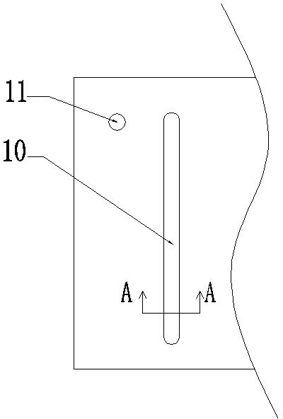
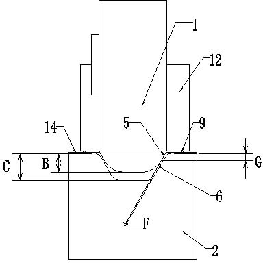
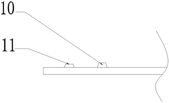
[0030] It should be noted that since both ends of the hypotenuse convex hull 10 are arc-shaped, it is special, so image 3 , Figure 4 It is a schematic diagram of the cross-sectional structure, and the cross-sections at the positions of the respective modules are the same as figure 1 The position of the A-A section in the corresponding, that is image 3 , Figure 4 The cross-sectional structure shown is the cross-sectional structure at the position shown in the A-A section of the processed hypotenuse convex hull 10 other than both ends, and the shown section is parallel to the A-A section.

[0031] refer to figure 1 and figure 2 As shown, the stamping die of the present invention mainly includes two modules: a first module and a second module.

[0032] Among them, refer to image 3 As shown, the first die set includes: a first pu...


PUM


Abstract

The invention claims a punching mould of LCD (liquid crystal display) flat-panel display back plane bevel edge convex packet and a punching method, wherein the punching mould comprises a first module and a second module, the first module comprises a first punching head and a first lower template, the first lower template is provided with a first forming groove which is sunk, the second module comprises a second punching head and a second lower template, the second lower template is provided with a second forming groove which is sunk; the punching method of the invention using the punching mould comprises the following steps: punching materials with the first module to form a middle convex packet; performing back processing to the middle convex packet with the second module to form a target convex packet; the punching mould and the punching disclosed by the invention have the advantages of using two sets of modules to reduce the torsion of the material caused by forming, and using a nitrogen spring and a pressure line to increase material pressing force caused by punching and forming and to prevent pulling the materials on the plane to make the plane rebound.

Description

technical field [0001] The invention relates to a stamping die and a stamping method, in particular to a stamping die and a stamping method for a beveled convex hull of an LCD flat panel display, and belongs to the field of stamping dies. Background technique [0002] LCD display technology has achieved rapid development in recent years, which has led to the simultaneous growth of the related LCD display backplane industry. LCD display backplane is a product with high technical content, such as product distortion, edge shaking, local rebound, etc. Especially for a large-size LCD display backplane, the technical difficulties of stamping include: product distortion And the local rebound index is kept within a certain error range, which also means that higher requirements are put forward for the stamping die. [0003] like figure 1 , figure 2 As shown in , the hypotenuse convex hull 10 is an important structure in the backplane of the LED display. Compared with the circular...

Claims


Application Information

Patent Timeline
Patent Type & Authority Applications(China)
IPC IPC(8): B21D37/10B21D22/02
Inventor 许一青
Owner KUNSHAN SANJING SCI & TECH
Why Eureka
Try Eureka