Light emitting diode packaging structure and manufacturing method of light emitting diode packaging structure

A technology for light-emitting diodes and packaging structures, applied in electrical components, electrical solid-state devices, circuits, etc., can solve the problems of large substrate thickness, low yield, and complex packaging structure.

Inactive Publication Date: 2012-07-25
ZHANJING TECH SHENZHEN +1
View PDF2 Cites 0 Cited by
  • Summary
  • Abstract
  • Description
  • Claims
  • Application Information

AI Technical Summary

Problems solved by technology

[0002] Most of the current light emitting diode (Light Emitting Diode, LED) packaging structure is to form a reflective cup on the substrate, and the reflective cup is formed by recessing from one surface of the substrate to the other surface. The depth is at least greater than the thickness of the light-emitting diode, and the thickness of the reflective cup on the substrate is usually set within a certain range to ensure sufficient strength to support the light-emitting diode in the reflective cup. Therefore, the substrate in this light-emitting diode packaging structure The thickness of the light-emitting diode packaging structure is relatively large, resulting in a large thickness of the packaged light-emitting diode packaging structure
For some thinner LED packaging structures, for example, a through hole is provided on the substrate, and an electrode layer is provided on the outside of the substrate to support the LED located in the through hole. In order to ensure sufficient support strength, it is often necessary to install There are at least two or more electrode layers, resulting in a complex package structure, and setting multi-layer electrode layers will lead to a very complicated manufacturing process and low yield

Method used


Image

  • Light emitting diode packaging structure and manufacturing method of light emitting diode packaging structure
  • Light emitting diode packaging structure and manufacturing method of light emitting diode packaging structure
  • Light emitting diode packaging structure and manufacturing method of light emitting diode packaging structure

Examples


Embodiment Construction

[0034] The present invention will be further described in detail below in conjunction with the accompanying drawings.

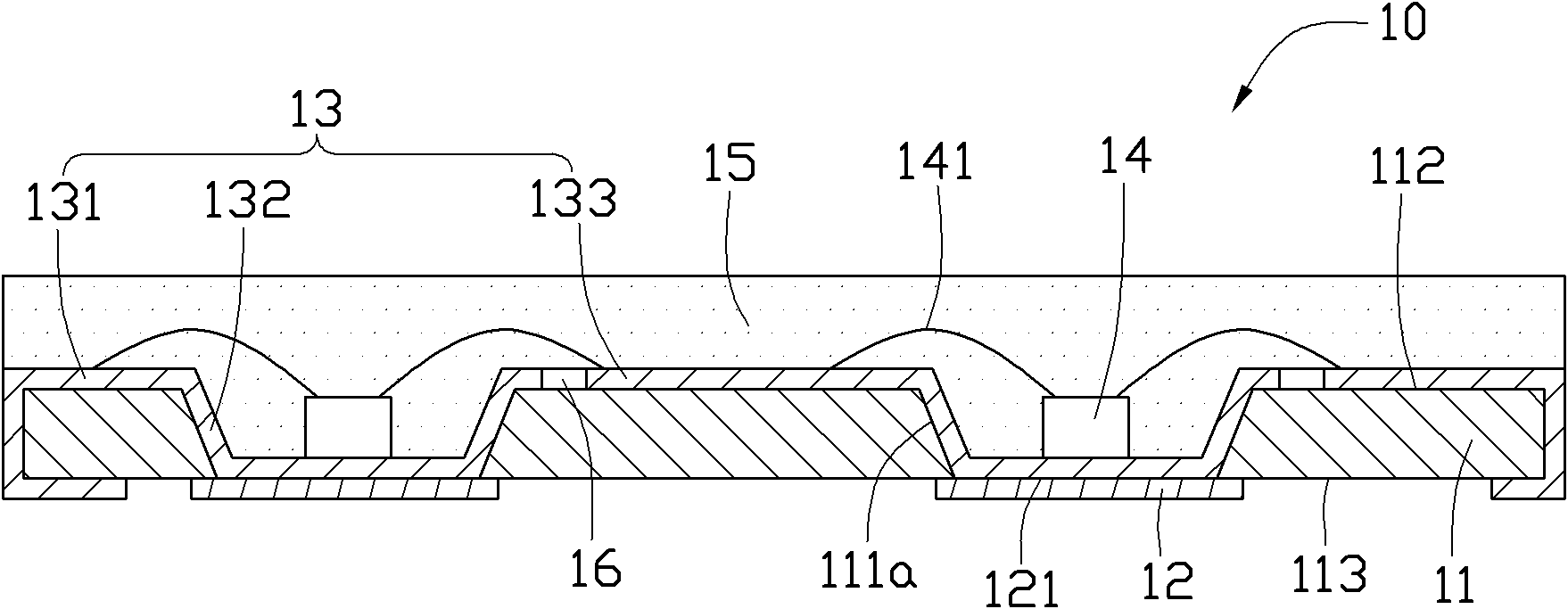
[0035] see figure 1 , The first embodiment of the present invention provides a LED packaging structure 10 , which includes a substrate 11 , several support plates 12 , an electrode layer 13 , several LED chips 14 and a packaging layer 15 .

[0036] see Figure 4 , the substrate 11 is in the shape of a plate, and a through hole 111 is formed on the substrate 11 , and the substrate includes a first surface 112 and a second surface 113 opposite to each other. The substrate 11 is used to support the LED packaging structure 10 . The through hole 111 is bounded by an inclined side surface 111 a and penetrates downwardly from the first surface 112 of the substrate 11 to the second surface 113 of the substrate 11 . The material of the substrate 11 is bismaleimide triazine resin (Bismaleimide Triazine resin, BT resin) or epoxy glass cloth. The thickness of the sub...


PUM


Abstract

The invention relates to a light emitting diode packaging structure. The light emitting diode packaging structure comprises base plates, an electrode layer, light emitting diode chips and a packaging layer. Communicated through holes are arranged in the base plates, and the light emitting diode packaging structure also comprises support plates arranged at one sides of the through holes in a covering manner. The electrode layer is plated on the surfaces of the base plates and the support plates. The light emitting diode chips are arranged in the through holes, are positioned on the support plates and are electrically connected with the electrode layer through the metal leads. The packaging layer covers the light emitting diode chips and the metal leads. The invention also relates to a manufacturing method of the light emitting diode packaging structure.

Description

technical field [0001] The invention relates to a semiconductor structure, in particular to a light emitting diode packaging structure and a manufacturing method thereof. Background technique [0002] Most of the current light emitting diode (Light Emitting Diode, LED) packaging structure is to form a reflective cup on the substrate, and the reflective cup is formed by recessing from one surface of the substrate to the other surface. The depth is at least greater than the thickness of the light-emitting diode, and the thickness of the reflective cup on the substrate is usually set within a certain range to ensure sufficient strength to support the light-emitting diode in the reflective cup. Therefore, the substrate in this light-emitting diode packaging structure The thickness of the light-emitting diode is relatively large, resulting in a relatively large thickness of the packaged light emitting diode packaging structure. For some thinner LED packaging structures, for exam...

Claims


Application Information

Patent Timeline
Patent Type & Authority Applications(China)
IPC IPC(8): H01L33/48H01L33/54H01L33/62H01L33/60H01L25/13H01L33/00
CPCH01L33/52H01L25/0753H01L33/486H01L33/641H01L33/62H01L2224/48091H01L33/60H01L2933/0033H01L2924/00012H01L2924/00014
Inventor 陈滨全林新强曾文良
Owner ZHANJING TECH SHENZHEN
Why Eureka
Try Eureka