A back-contact silicon cell, its non-light-receiving surface treatment method, and its preparation method

A technology of crystalline silicon cells and light-receiving surfaces, which is applied in circuits, photovoltaic power generation, electrical components, etc., can solve the problems of low photoelectric conversion efficiency of crystalline silicon cells, and achieve the goal of increasing photoelectric conversion efficiency, improving utilization efficiency, and high photoelectric conversion efficiency Effect

Active Publication Date: 2016-04-20
紫石能源有限公司
View PDF8 Cites 0 Cited by
  • Summary
  • Abstract
  • Description
  • Claims
  • Application Information

AI Technical Summary

Problems solved by technology

[0005] Therefore, the technical problem to be solved by the present invention is to overcome the defect of low photoelectric conversion efficiency of crystalline silicon cells in the prior art, thereby providing a back contact crystalline silicon cell with high photoelectric conversion efficiency

Method used


Image

  • A back-contact silicon cell, its non-light-receiving surface treatment method, and its preparation method
  • A back-contact silicon cell, its non-light-receiving surface treatment method, and its preparation method
  • A back-contact silicon cell, its non-light-receiving surface treatment method, and its preparation method

Examples


Embodiment 1

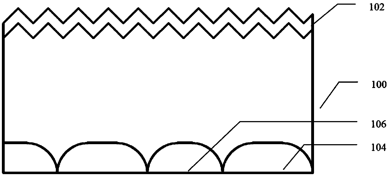
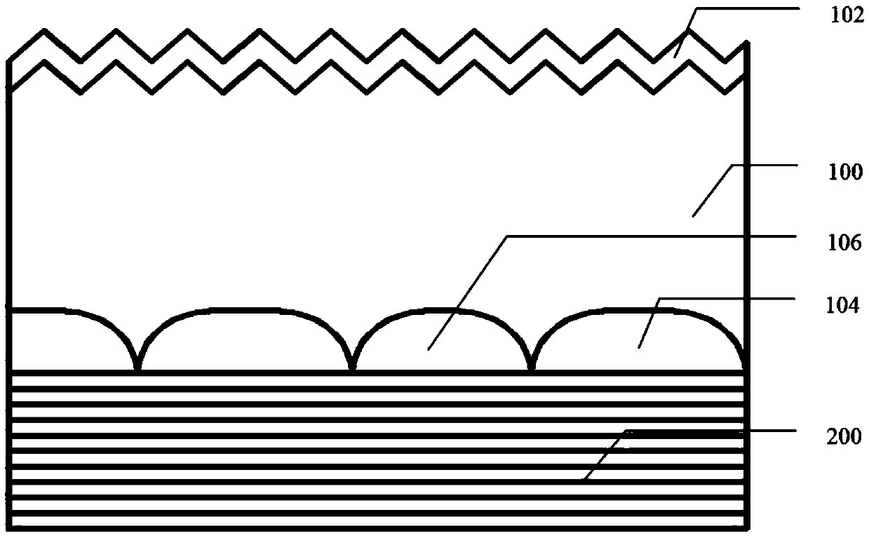
[0056] This embodiment provides a back contact crystalline silicon battery, such as Figure 2-4 As shown, a silicon substrate 100 is included. The silicon substrate 100 has a light-receiving surface and a non-light-receiving surface. On the non-light-receiving surface, a P-type region busbar conductive strip 108 and an N-type region busbar conductive strip 112 are arranged in a PNPN type. In an arrangement structure, the P-type region bus conductive tape 108 is connected to the positive metal electrode 110, and the N-type region bus conductive tape 112 is connected to the negative metal electrode, covering the P-type region bus conductive tape 108 and the N-type region The bus conductive strip 112 is arranged on the five-layer Bragg reflective layer 200 on the non-light-receiving surface, the Bragg reflective layer 200 is arranged along the thickness direction of the crystalline silicon cell, and each layer of the Bragg reflective layer 200 includes a first A first Bragg reflec...

Embodiment 2

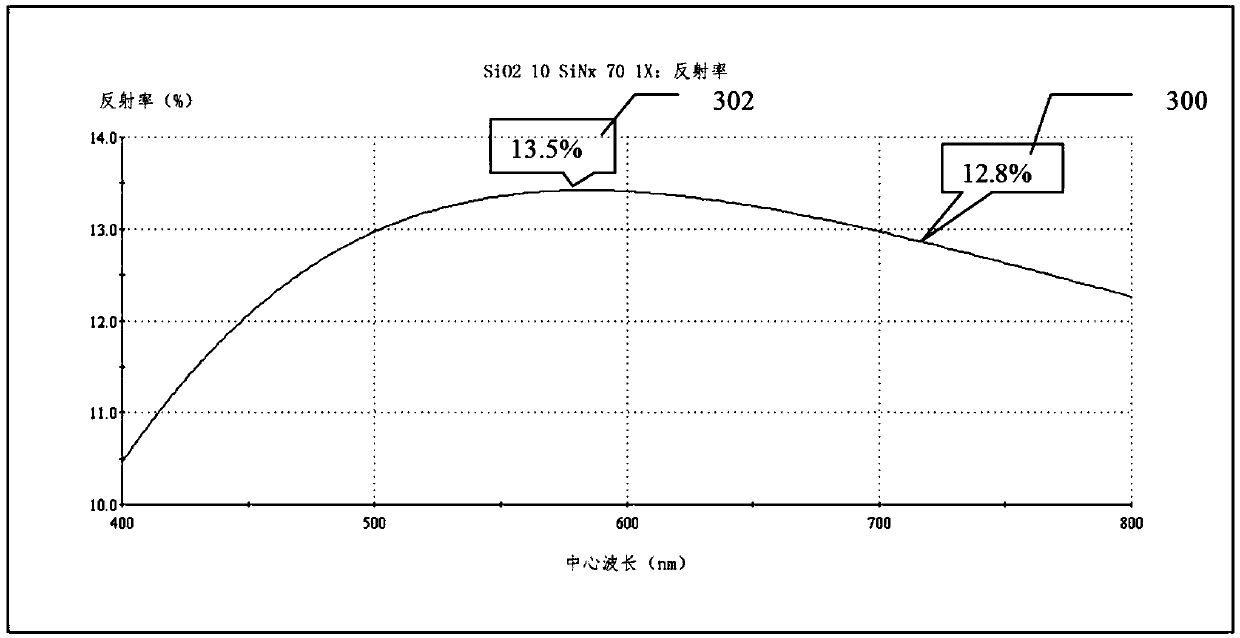
[0060] This embodiment provides a back contact crystalline silicon cell, which is a modification on the basis of Embodiment 1. The difference is that in this embodiment, light with a central wavelength λ=600nm is taken as the target reflected light, and the formula d1=d2 =1 / 8λ calculates d1=d2=75nm. According to this data, 5 layers of the above-mentioned Bragg reflective layer 200 are deposited on the non-light-receiving surface. The data obtained by the test is as follows Image 6 As shown, the maximum reflectivity 302 for light with a wavelength in the range of 400-800nm ​​is 65%, and the average reflectivity 300 is 30%, and Figure 5 The data in is not much different, but the reflection effect is greatly enhanced compared with the reflection effect of the existing passivation layer.

[0061] As a modification of this embodiment, the above-mentioned Bragg reflective layer 200 can be provided with 2-8 layers, which can achieve the purpose of the invention.

Embodiment 3

[0063] This embodiment provides a back contact crystalline silicon battery, which is a modification on the basis of Embodiment 1. The difference is that the first material in this embodiment is SiO 2 , The thickness of the first Bragg reflective film formed by it is d1, and the second material is TiO 2 , The thickness of the second Bragg reflective film formed by it is d2, where SiO 2 Refractive index n 1 =1.46, TiO 2 Refractive index n 2 =2.35.

[0064] Take the center wavelength as λ 1 =500nm and λ 2 =800nm ​​light is reflected by two targets, and through the formula d1=(2λ 1 -λ 2 ) / (2n 1 ), d2=(λ 2 -λ 1 ) / (2n 2 ) Respectively calculated d1=68.2nm, d2=78.9nm. According to this data, 5 layers of the above-mentioned Bragg reflective layer 200 are deposited on the non-light-receiving surface. The measured data are as follows Figure 7 As shown, the maximum reflectance 302 for light with a wavelength in the range of 400-800 nm is 93%, and the average reflectance 300 is about 50%, and ...


PUM


Abstract

The invention provides a back contact crystalline silicon battery, a treatment method for a non-illuminated surface of the back contact crystalline silicon battery and a preparation method for the back contact crystalline silicon battery. The back contact crystalline silicon battery comprises a silicon substrate, wherein the silicon substrate is provided with an illuminated surface and the non-illuminated surface; P-type region confluence conductive strips and N-type region confluence conductive strips are arranged on the non-illuminated surface to form a P-N-P-N type arrangement structure; the P-type region confluence conductive strips are connected with a positive metal electrode; the N-type region confluence conductive strips are connected with a negative metal electrode; therefore, 2-8 bragg reflection layers of the P-type region confluence conductive strips and the N-type region confluence conductive strips, which are arranged on the non-illuminated surface, can be covered; the bragg reflection layers are arranged along the thickness direction of the crystalline silicon battery; each bragg reflection layer comprises a first bragg reflection film made of a first material and a second bragg reflection film made of a second material; the first bragg reflection films and the second bragg reflection films are stacked in a staggered manner along the thickness direction of the crystalline silicon battery; the reflectivity n2 of the second material is higher than the reflectivity n1 of the first material.

Description

Technical field [0001] The invention relates to a back contact crystalline silicon battery and a method for processing its non-light-receiving surface and a preparation method thereof, belonging to the technical field of crystalline silicon solar cells. Background technique [0002] The solar photovoltaic power generation industry is developing very rapidly. Since 2007, China's photovoltaic production has been the world's first. Its product types are mainly crystalline silicon cells and modules, occupying nearly 90% of the market. Although China's photovoltaic manufacturing volume is the first, the photoelectric conversion efficiency of photovoltaic products is at an intermediate level. [0003] Crystalline silicon solar cell is a kind of solar cell, whose main function is to convert the sun's light energy into electric energy. Crystalline silicon solar cells receive photons from the sun to generate carriers, and carry out recombination of carriers. When the carrier recombination...

Claims


Application Information

Patent Timeline
Patent Type & Authority Patents(China)
IPC IPC(8): H01L31/0216H01L31/18
CPCH01L31/02168H01L31/0682H01L31/1804Y02E10/547Y02P70/50
Inventor 顾世海张庆钊兰立广丁建
Owner 紫石能源有限公司
Why Eureka
Try Eureka