Array substrate and manufacturing method thereof, and display apparatus

An array substrate, substrate technology, applied in the field of array substrate and its manufacturing method and display device, can solve the problems of affecting the quality of OTFT, affecting the quality of OTFT liquid crystal display, difficult to accurately control the size of ink droplets, etc.

Active Publication Date: 2012-08-08
BOE TECH GRP CO LTD
View PDF4 Cites 21 Cited by
  • Summary
  • Abstract
  • Description
  • Claims
  • Application Information

AI Technical Summary

Problems solved by technology

[0004] During the printing process, it is difficult to precisely control the size of the ink drop due to the surface tension of the ink drop, which makes it difficult to accurately control the shape of the OTFT source and drain formed by the inkjet printing process, thereby affecting the quality of the OTFT. This will affect the quality of OTFT liquid crystal display

Method used


Image

  • Array substrate and manufacturing method thereof, and display apparatus
  • Array substrate and manufacturing method thereof, and display apparatus
  • Array substrate and manufacturing method thereof, and display apparatus

Examples


Embodiment Construction

[0049] The following will clearly and completely describe the technical solutions in the embodiments of the present invention with reference to the accompanying drawings in the embodiments of the present invention. Obviously, the described embodiments are only some, not all, embodiments of the present invention. Based on the embodiments of the present invention, all other embodiments obtained by persons of ordinary skill in the art without making creative efforts belong to the protection scope of the present invention.

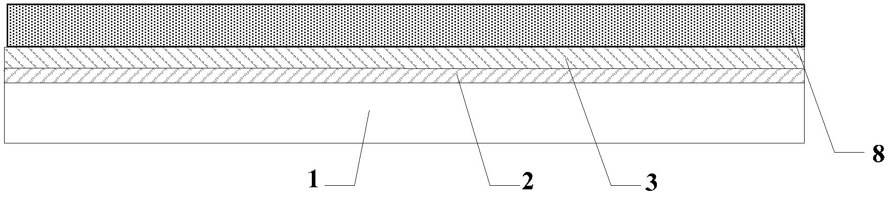
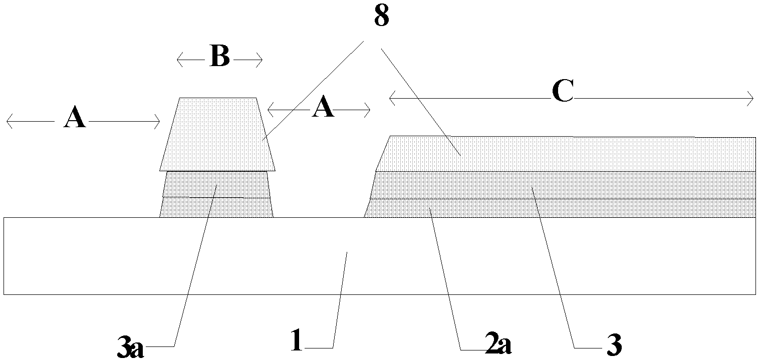
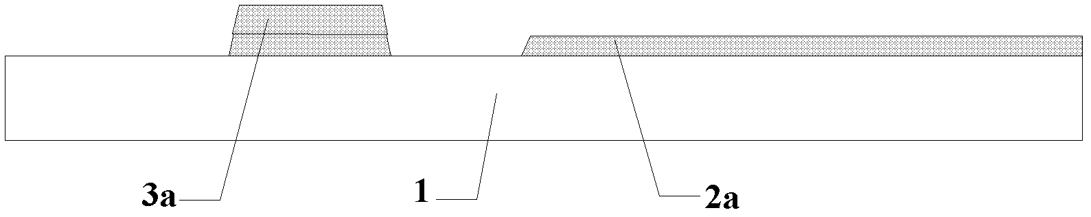
[0050] An embodiment of the present invention provides an array substrate, such as Figure 12As shown, it includes: a substrate 1, a pixel structure formed on the substrate 1; the pixel structure includes: a gate line, a data line, a thin film transistor and a pixel electrode 11a; the thin film transistor includes a gate 3a, a gate insulating layer 4, and an active layer 9 , source 6, drain 7, wherein, gate 3a is electrically connected with described gate line...


PUM


Abstract

The invention discloses an array substrate and a manufacturing method thereof, and a display apparatus and relates to the display technology field. The invention aims at accurately control shapes of a source electrode and a drain electrode of a TFT (thin film transistor). The array substrate comprises a pixel structure formed on the substrate. The pixel structure comprises a grid line, a data line, the TFT and a pixel electrode. The TFT comprise a grid, a gate insulation layer, an active layer, the source electrode and the drain electrode, wherein the grid is electrically connected with the grid line, the source electrode is electrically connected with the data line, and the drain electrode is electrically connected with the pixel electrode. The pixel structure also comprises an organic insulating layer which is located above the gate insulation layer and is an E-shape structure at the position of the TFT. The source electrode and the drain electrode of the TFT are located on two valleys of the E-shape structure respectively. The scheme of the invention is suitable for production manufacturing of a liquid crystal display panel and a liquid crystal display.

Description

technical field [0001] The invention relates to the field of manufacturing liquid crystal displays, in particular to an array substrate, a manufacturing method thereof, and a display device. Background technique [0002] Organic thin film transistors (Organic Thin Film Transistor, hereinafter referred to as OTFT) have the advantages of being suitable for large-area processing and being suitable for flexible substrates, and have shown application prospects in the field of flat panel displays. Therefore, the research and development of OTFT array substrates has received extensive attention. Usually, multiple patterning processes are required in the manufacture of the OTFT array substrate to form a patterned layer structure. At present, there is an inkjet printing process to prepare the source and drain electrodes of OTFT. Among them, the inkjet printing process is a process of printing the material melt (ie, ink droplet) used for making patterns on the area where the pattern...

Claims


Application Information

Patent Timeline
Patent Type & Authority Applications(China)
IPC IPC(8): H01L51/05H01L29/786H01L21/77G02F1/1368
CPCH01L27/307H01L27/1248H01L29/78696H01L51/0545H01L29/7869H01L29/4908H01L29/42384H01L29/786H01L29/41733H10K39/32H10K10/466
Inventor 张学辉
Owner BOE TECH GRP CO LTD
Why Eureka
Try Eureka