Metamaterial with dielectric substrate with nonuniform thickness

A technology of dielectric substrates and metamaterials, applied in the field of metamaterials, can solve problems such as high production costs, artificial microstructure design of complex manufacturing processes, etc., and achieve the effects of simple process design, rich functional applications, and low production costs

Active Publication Date: 2012-08-15
KUANG CHI INST OF ADVANCED TECH
View PDF5 Cites 6 Cited by
  • Summary
  • Abstract
  • Description
  • Claims
  • Application Information

AI Technical Summary

Problems solved by technology

[0003] In order to realize the electromagnetic function of existing metamaterials, it is necessary to assemble multiple layers of dielectric substrates with artificial microstructures in various arrangements. On the one hand, it requires high production costs, and on the other hand, it needs to adopt complex manufacturing processes. Structural design and fine processing of artificial microstructures

Method used


Image

  • Metamaterial with dielectric substrate with nonuniform thickness
  • Metamaterial with dielectric substrate with nonuniform thickness
  • Metamaterial with dielectric substrate with nonuniform thickness

Examples


Embodiment 1

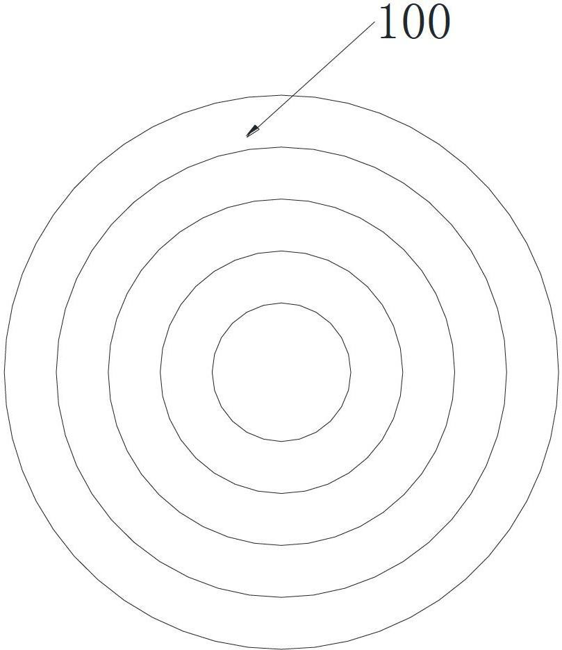
[0025] A metamaterial with a non-uniform thickness dielectric substrate, the overall structure of the metamaterial can be found in the attached figure 1 , including a stacked multilayer dielectric substrate 100 and a plurality of artificial microstructures 200 arranged on the dielectric substrate. For the structural diagram of the dielectric substrate 100, refer to the attached figure 2 , one side of the dielectric substrate 100 is convex ellipsoid, and the other side is flat, and the artificial microstructure 200 is arrayed on the flat side of the dielectric substrate 100 .

[0026] For metamaterials, we can regard the artificial microstructure, the dielectric substrate occupied by the artificial microstructure, and the space around them as a tiny unit that can generate electromagnetic responses to electromagnetic waves. The entire metamaterial is composed of many tiny units. By designing the structural shape of the artificial microstructures 200 in each tiny unit and orderl...

Embodiment 2

[0029] A metamaterial with a non-uniform thickness dielectric substrate, the overall structure of the metamaterial can be found in the attached image 3 , including a stacked multilayer dielectric substrate 100 and a plurality of artificial microstructures 200 arranged on the dielectric substrate. For the structural diagram of the dielectric substrate 100, refer to the attached Figure 4 , one side of the dielectric substrate 100 is concave ellipsoid, and the other side is flat, and the artificial microstructure 200 is arrayed on the flat side of the dielectric substrate 100 .

[0030] According to the above design principles and ideas, in this embodiment, by designing the dielectric substrate 100 as a concave ellipsoid similar to a concave lens, the electromagnetic waves passing through the dielectric substrate can have a diverging effect, so that the metamaterial can obtain electromagnetic wave divergence on the basis of the original functional characteristics. function to i...

Embodiment 3

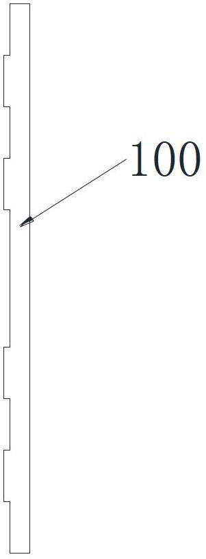
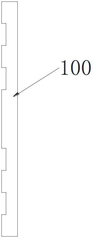
[0032] As a modification of the above-mentioned embodiment, the present invention can also design the dielectric substrate 100 as the following structure, refer to the attached Figure 5 And attached Image 6 , with Figure 5 is a cross-sectional view of the dielectric substrate 100, Image 6 It is a side view of the dielectric substrate 100. One side of the dielectric substrate 100 is in the shape of a boss, and the other side is in the shape of a plate. The artificial microstructure 200 is arrayed on the plate-shaped side of the dielectric substrate 100. Viewed from the side of the boss-shaped structure, the dielectric substrate 100 is back shape.

[0033] According to the above-mentioned design principles and ideas, in this embodiment, the equivalent permittivity and equivalent magnetic permeability of each back-shaped structure of the metamaterial are distributed in a ladder shape. On the one hand, by designing the structural shape and According to the arrangement rules...


PUM


Abstract

The invention provides a metamaterial with a dielectric substrate with nonuniform thickness, which comprises a multilayer dielectric substrate and multiple artificial microstructures, wherein the multiple artificial microstructures are arranged on the dielectric substrate; and the metamaterial is characterized in that the thickness of the dielectric substrate is distributed nonuniformly. The metamaterial disclosed by the invention has the advantages that through designing the thickness of the dielectric substrate into a nonuniformly-distributed mode, the metamaterial has more abundant function applications; and as a concrete implementation mode of the metamaterial disclosed by the invention, the convergence, divergence and deflection effects of the metamaterial on electromagnetic waves can be achieved through the nonuniform distribution of the thickness, so that the metamaterial is simpler in process design and lower in production cost.

Description

【Technical field】 [0001] The invention relates to the field of metamaterials, in particular to a metamaterial with a non-uniform thickness dielectric substrate. 【Background technique】 [0002] The basic structure of metamaterials includes a multi-layer dielectric substrate and multiple artificial microstructures arranged on the dielectric substrate. The thickness of the dielectric substrate of the existing metamaterials is uniform in thickness. The realization of the function of the metamaterial is mainly by changing the array in the medium The structure of the artificial microstructure on the substrate, through the precise design and control of the artificial microstructure, can make the metamaterial exhibit various electromagnetic properties, such as the ability to converge, diverge and deflect electromagnetic waves, etc., and the dielectric substrate is the main body of the metamaterial Components have little to no function. [0003] In order to realize the electromagnet...

Claims


Application Information

Patent Timeline
Patent Type & Authority Applications(China)
IPC IPC(8): H01Q15/00G02B3/08
Inventor 刘若鹏赵治亚孙豪文
Owner KUANG CHI INST OF ADVANCED TECH
Why Eureka
Try Eureka