

Liquid crystal display device
A technology of liquid crystal display device and liquid crystal layer, which is applied in static indicators, instruments, nonlinear optics, etc., can solve the problems of device structure limitation and the difficulty of integrating multiple liquid crystal driving methods, etc., so as to improve application occasions and good adaptability Effect
- Summary
- Abstract
- Description
- Claims
- Application Information
AI Technical Summary
Problems solved by technology
Method used
Image

Examples
Embodiment 1
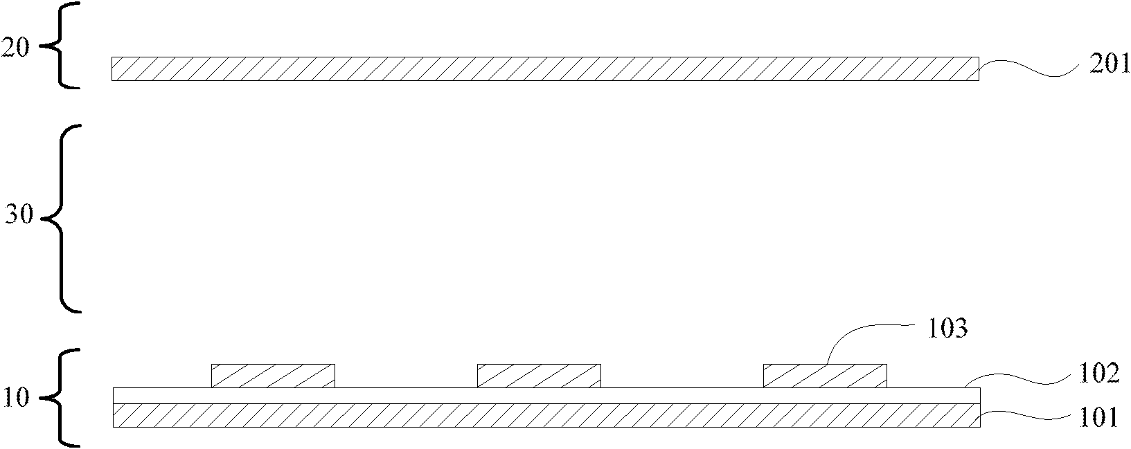
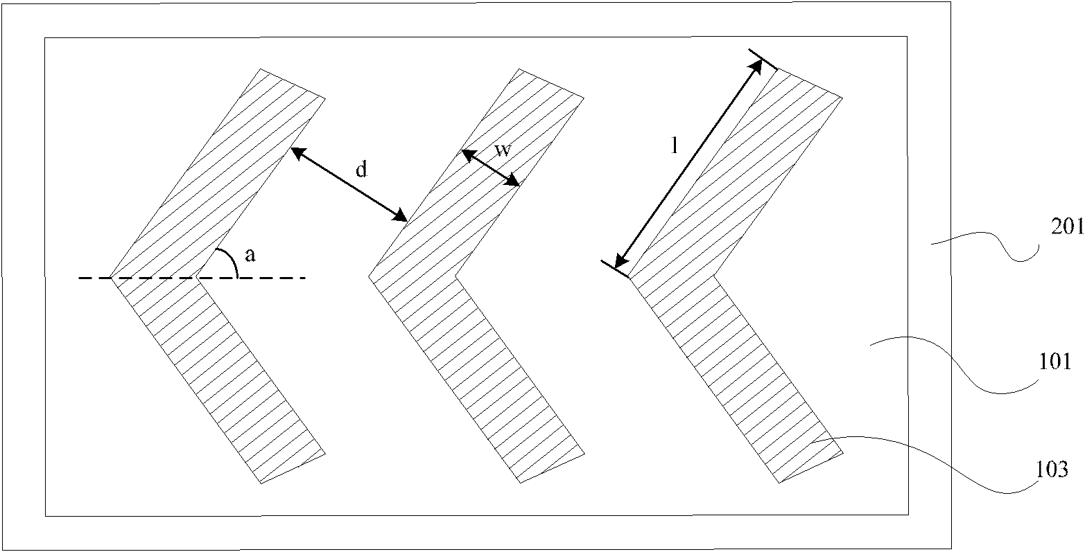
[0048] As mentioned in the background technology section, in the same liquid crystal display device in the prior art, there is generally only one liquid crystal driving mode. In order to solve this problem, the embodiment of the present invention provides a liquid crystal display that can work in two working modes device, the liquid crystal display device includes a plurality of pixel structures, wherein a cross-sectional view of a pixel structure is shown in figure 1 As shown, the top view is as figure 2 As shown, the liquid crystal display device includes the following components:
[0049] The first substrate 10 and the second substrate 20 arranged oppositely;
[0050] a positive liquid crystal layer 30 disposed between the first substrate 10 and the second substrate 20;
[0051] The first substrate 10 includes at least a first transparent substrate (not shown in the figure, specifically a glass substrate may be used), a first common electrode 101 located on the side of t...
Embodiment 2
[0061] The structure of the liquid crystal display device disclosed in this embodiment is the same as that of the previous embodiment. The difference is that this embodiment is based on the previous embodiment, combined with specific electric field conditions, potential conditions, and the arrangement of liquid crystals corresponding to different electric fields. The operating principle of the liquid crystal display device will be described in detail.
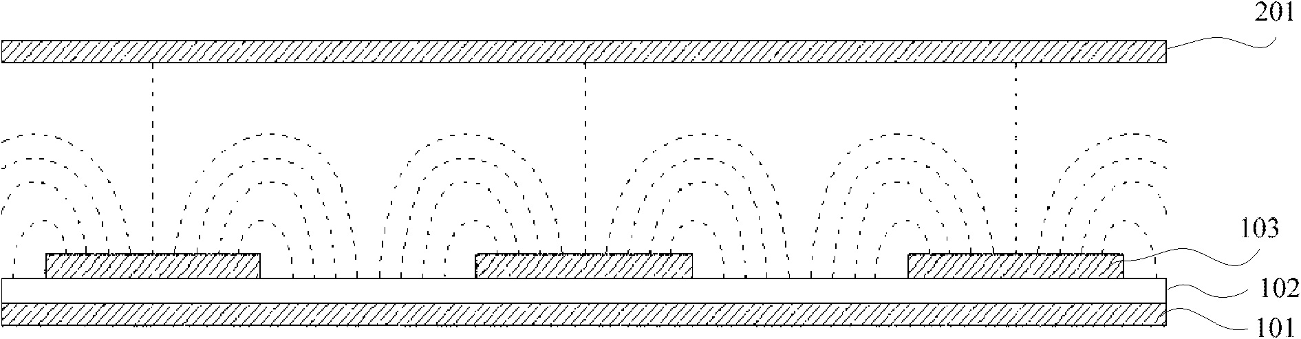
[0062] The liquid crystal display device disclosed in the embodiment of the present invention can work in the transmissive working mode and the reflective working mode, combined below Figure 3-Figure 5 The distribution of electric field lines in different working modes is shown, and the specific working mode of the liquid crystal display device is described in detail.
[0063] The liquid crystal display device works in the transmission mode when the external light is weak. In the transmission mode, the FFS driving method is ad...
Embodiment 3
[0082] In order to realize the potential control of each electrode of the liquid crystal display device, the first substrate in the liquid crystal display device disclosed in this embodiment further includes a plurality of gate lines and a plurality of data lines, and the plurality of gate lines and a plurality of data lines Lines intersect perpendicularly, defining pixel units;
[0083] A thin film transistor (TFT, Thin Film Transistor) is disposed on the side of the first substrate facing the liquid crystal layer. The thin film transistor is located at the intersection of the gate line and the data line and can be used as a switch of the pixel unit.
[0084] Wherein, in this embodiment, each pixel unit has a thin film transistor.
[0085] In addition, the first substrate further includes: a first polarizer located on a side of the first substrate facing away from the liquid crystal layer, the absorption axis of the first polarizer is oriented in the same direction as that in...
PUM
 Abstract
Description
Claims
Application Information