Pixel unit, array substrate, liquid crystal panel, display device and manufacturing methods thereof

A technology for pixel units and array substrates, which is applied in semiconductor/solid-state device manufacturing, transistors, electrical components, etc., and can solve the problems of small aperture ratio and inability to meet high-quality display.

Active Publication Date: 2012-08-22
BOE TECH GRP CO LTD
View PDF5 Cites 35 Cited by
  • Summary
  • Abstract
  • Description
  • Claims
  • Application Information

AI Technical Summary

Problems solved by technology

However, due to its own characteristics, the aperture ratio of traditiona

Method used


Image

  • Pixel unit, array substrate, liquid crystal panel, display device and manufacturing methods thereof
  • Pixel unit, array substrate, liquid crystal panel, display device and manufacturing methods thereof
  • Pixel unit, array substrate, liquid crystal panel, display device and manufacturing methods thereof

Examples


Embodiment 1

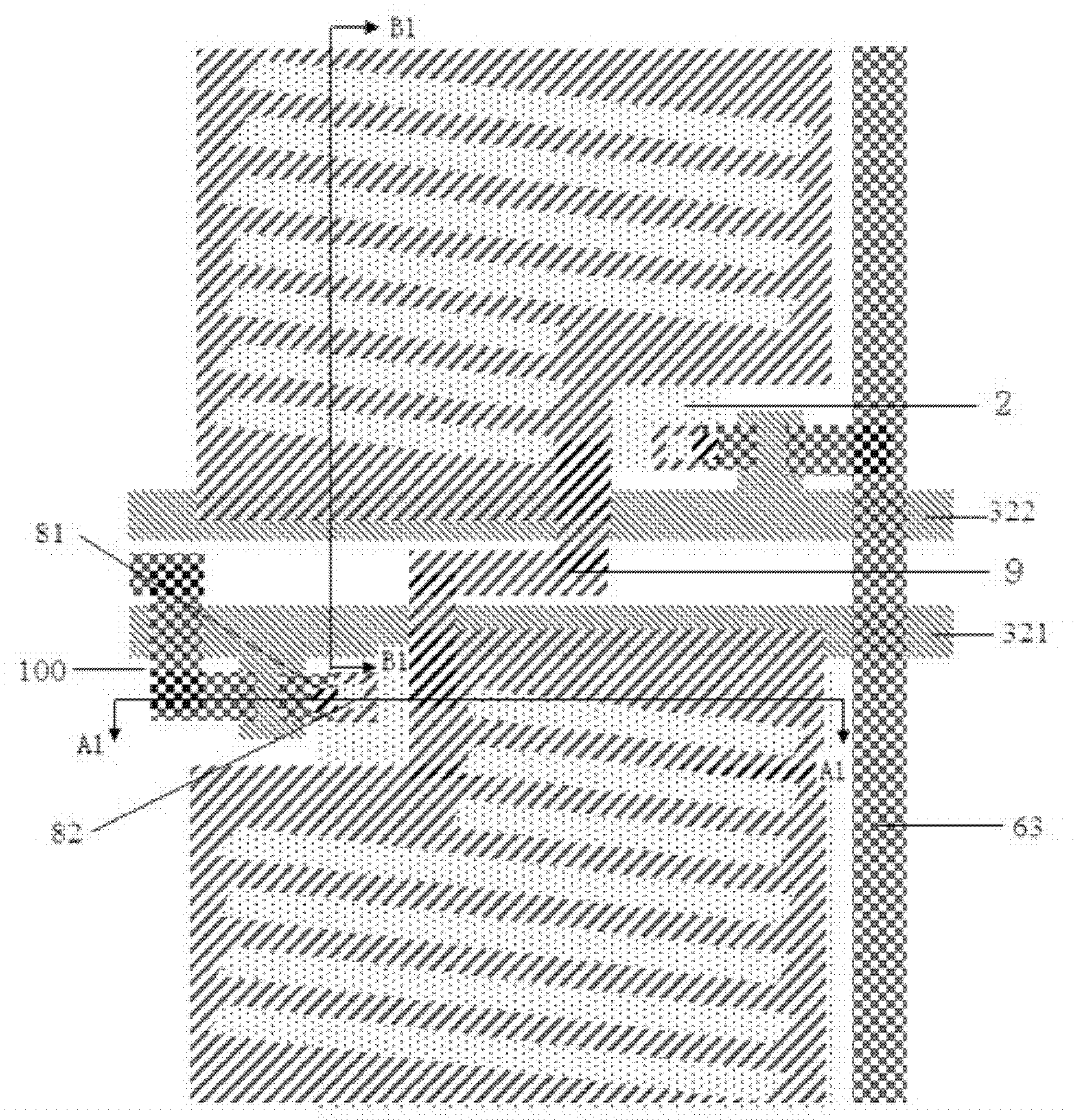
[0088] An embodiment of the present invention provides a pixel unit, the following refers to figure 1 with Figure 1A The structure of the pixel unit in this embodiment will be described. It should be clarified that the pixel unit defined in this embodiment does not include gate lines and data lines. The pixel unit can be used to form a common array substrate or a dual-gate array substrate after the gate lines and data lines are properly arranged.

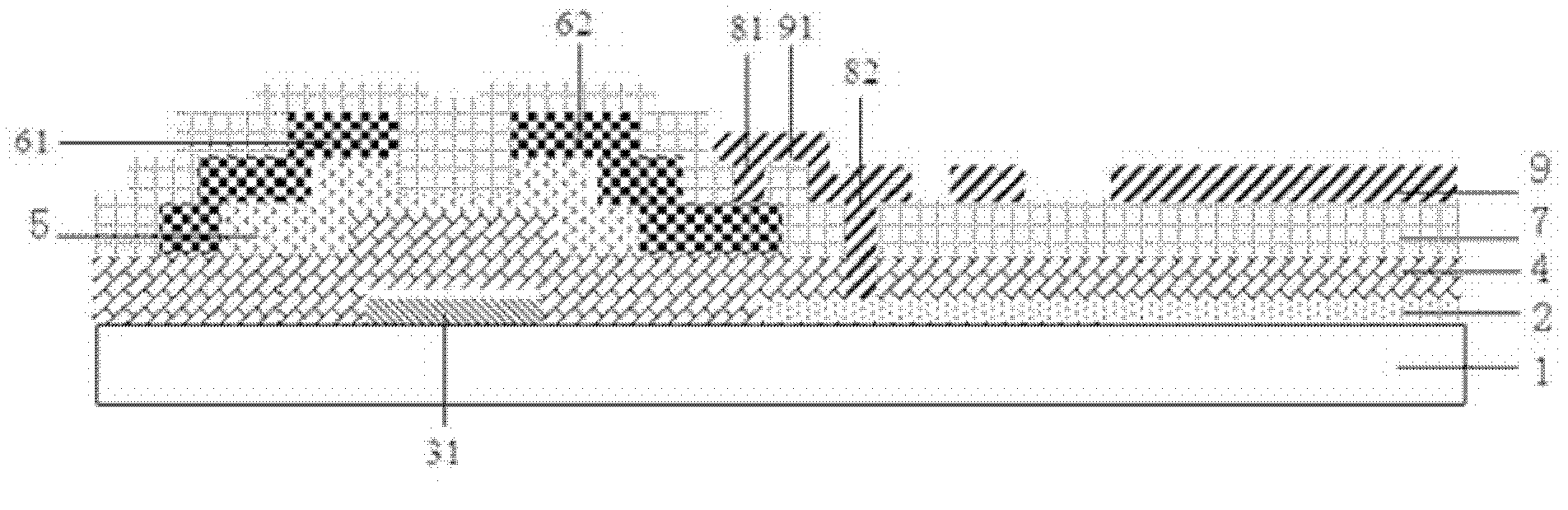
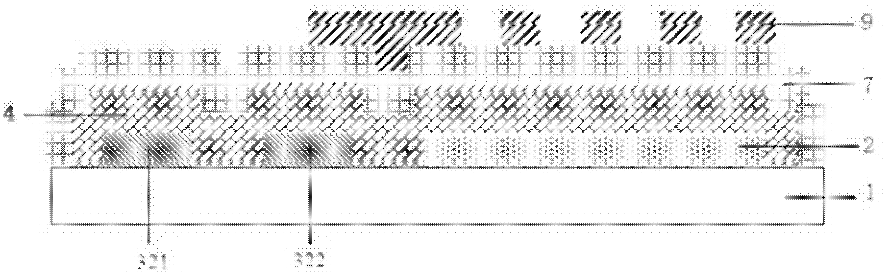
[0089] figure 1 Shown is a schematic plan view of the pixel unit in the embodiment of the present invention, which selects two pixel units that are adjacent up and down; Figure 1A shown as figure 1 The cross-sectional view in the direction of A1-A1, Figure 1B for figure 1 Schematic diagram of B1-B1 cross-section in middle, that is Figure 1A with Figure 1BIt is a cross-sectional schematic diagram of different cutting directions of a pixel unit. The pixel unit in this embodiment includes a thin film transistor 100, a pix...

Embodiment 2

[0098] This embodiment provides an array substrate, including a substrate, on which a gate line is arranged, a data line is arranged perpendicular to the gate line, a pixel area is defined between the gate line and the data line, and the The pixel area includes the pixel unit described in the first embodiment above (see figure 1 ), wherein the gate of the thin film transistor is connected to the gate line, and the source of the thin film transistor is connected to the data line. It should be pointed out that the array substrate including the above-mentioned pixel units can be called an I-ADS array substrate; compared with the traditional ADS array substrate, the upper and lower positional relationship between the pixel electrode 2 and the common electrode 9 has changed.

[0099] As an array substrate in this embodiment, it may be the following array substrate: on the array substrate, gate lines are arranged above and below a plurality of pixel units in each row, and gate lines...

Embodiment 3

[0107] This embodiment provides a method for manufacturing an array substrate, such as Figure 9 shown, including the following steps:

[0108] S101, forming a pattern including a pixel electrode through a first patterning process, and forming a pattern including a gate line and a thin film transistor gate through a second patterning process;

[0109] Alternatively, the first patterning process is used to form the pattern including the gate line and the thin film transistor gate, and the second patterning process is used to form the pattern including the pixel electrode.

[0110] S102, forming a pattern including a gate insulating layer, an active layer, a data line, and a source electrode and a drain electrode of a thin film transistor through a third patterning process.

[0111] S103, forming a pattern including a passivation layer through a fourth patterning process.

[0112] S104, forming a pattern including a common electrode through a fifth patterning process.

[0113...


PUM

PropertyMeasurementUnit
Widthaaaaaaaaaa
Widthaaaaaaaaaa
Widthaaaaaaaaaa

Abstract

The invention discloses a pixel unit, an array substrate, a liquid crystal panel, a display device and manufacturing methods thereof, relating to the technical field of liquid crystal display and aiming to improve a pixel aperture opening ratio, reduce the power consumption and improve the display effect. The pixel unit comprises a thin film transistor, a pixel electrode and a common electrode; the thin film transistor comprises a grid electrode, a grid insulating layer arranged on the grid electrode, an active layer arranged on the grid insulating layer, a source electrode and a drain electrode arranged on the active layer, and a passivation layer arranged on the source electrode and the drain electrode, wherein the common electrode is directly arranged on the passivation layer; and the pixel electrode is arranged below the passivation layer and is connected with the drain electrode of the thin film transistor. According to the array substrate, the liquid crystal panel, the display device and the manufacturing methods thereof, a visual angle can be improved, the power consumption is reduced, the aperture opening ratio is improved and further the display quality can be improved. The pixel unit, the array substrate, the liquid crystal panel and the display device can be used for liquid crystal display.

Description

technical field [0001] The invention relates to the technical field of liquid crystal display, in particular to a pixel unit, an array substrate, a liquid crystal panel, a display device and a manufacturing method thereof. Background technique [0002] Liquid Crystal Display (LCD) has the characteristics of small size, low power consumption, and no radiation, and has now occupied a dominant position in the field of flat panel display. Thin Film Transistor-Liquid Crystal Display (TFT-LCD) is currently the mainstream liquid crystal display, and its liquid crystal panel includes an array substrate and a color filter substrate. Wherein, a gate line is provided on the array substrate, a data line is provided perpendicular to the gate line, a pixel area is defined between the gate line and the data line, and a thin film transistor and a pixel electrode are provided in the pixel area, The gate of the thin film transistor is connected to the gate line, the source is connected to th...

Claims


Application Information

Patent Timeline
IPC IPC(8): G02F1/1362G02F1/1368G02F1/1335G02F1/13357G02F1/1333H01L27/02H01L29/786H01L21/77
CPCG02F1/134309H01L27/124G02F2201/40G02F1/134318G02F1/136218G02F1/1343G02F1/1368G02F1/1335G02F1/134381G02F1/136209
Inventor 金熙哲徐超
Owner BOE TECH GRP CO LTD
Why Eureka
Try Eureka