Packaging structure and manufacturing method thereof

A technology of packaging structure and manufacturing method, applied in semiconductor/solid-state device manufacturing, semiconductor/solid-state device components, semiconductor devices, etc., can solve the problems of high material cost, new manufacturing process, unsatisfactory reliability and heat dissipation performance, etc. , to achieve the effect of good reliability and heat dissipation performance, and low material cost

Active Publication Date: 2012-08-22
SAMSUNG SEMICON CHINA RES & DEV +1
View PDF5 Cites 6 Cited by
  • Summary
  • Abstract
  • Description
  • Claims
  • Application Information

AI Technical Summary

Problems solved by technology

[0007] The main problems of existing packages that do not use substrates with circuits are high material cost...

Method used


Image

  • Packaging structure and manufacturing method thereof
  • Packaging structure and manufacturing method thereof
  • Packaging structure and manufacturing method thereof

Examples


Embodiment Construction

[0027] The present invention is described more fully hereinafter with reference to the accompanying drawings, in which embodiments of the invention are shown. However, this invention may be embodied in many different forms and should not be construed as limited to the embodiments set forth herein. Rather, these embodiments are provided so that this disclosure will be thorough and complete, and will fully convey the scope of the invention to those skilled in the art. In the drawings, the size and relative sizes of layers and regions may be exaggerated for clarity.

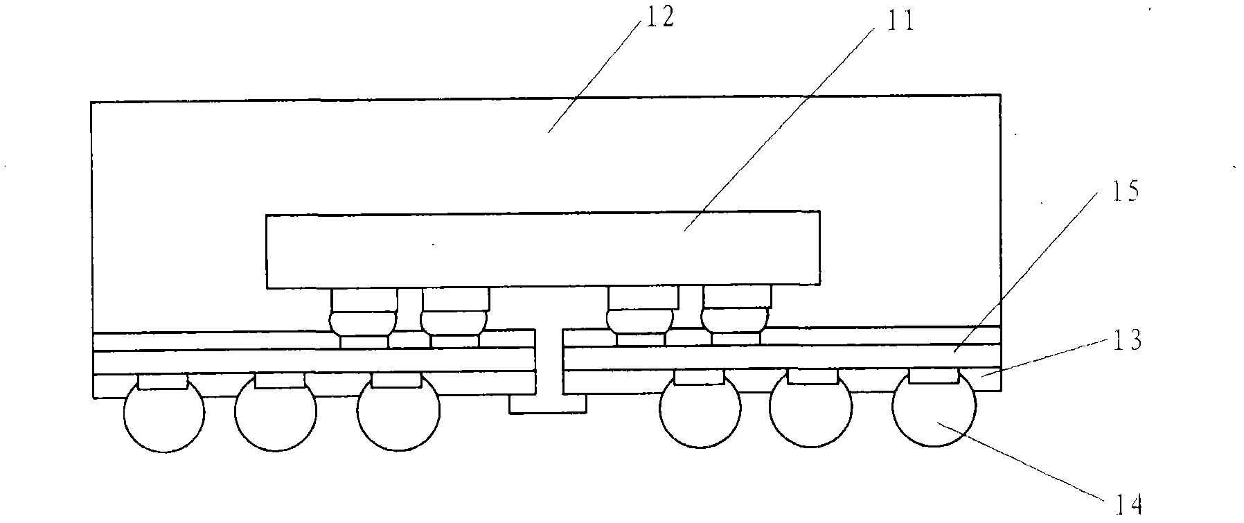
[0028] Figure 4 is a schematic diagram illustrating a package structure of a thermally conductive carrier board with high thermal conductivity according to an exemplary embodiment of the present invention.

[0029] refer to Figure 4 , according to one aspect of the present invention, a package structure is provided, the package structure includes: a heat conduction carrier 43, formed by a material with high the...


PUM


Abstract

The invention provides a packaging structure for a thermal conductive carrier board with high thermal conductivity and a manufacturing method thereof. The packaging structure comprises a thermal conductive carrier board, a chip, bumps, a plastic package material, a conductive material and an insulation material. The manufacturing method comprises the steps of preparing the chip; forming bumps on the chip; plastically packaging the chip provided with bumps by the plastic package material; exposing the bumps; forming a circuit pattern on the plastic package material; filling circuit pattern with the conductive material to be electrically connected with the bumps; covering the bumps and the conductive material with the insulation material, and exposing one end of the conductive material so as to electrically connect the chip with outside. The packaging structure and the manufacturing method thereof provided by the utility model have the advantages of low material cost, good reliability and heat dissipation and no new device is required for the manufacturing method.

Description

technical field [0001] The present invention relates to a semiconductor packaging structure and a manufacturing method thereof, and more particularly, the present invention relates to a semiconductor packaging structure that does not use a substrate with a circuit (such as a printed circuit board (PCB)) but uses a heat-conducting carrier board with high thermal conductivity. Package structure and manufacturing method thereof. Background technique [0002] With the rapid development of the semiconductor industry and its rapid penetration into various industries, electronic packaging has gradually become a bottleneck in the realization of the functions of semiconductor chips. Therefore, electronic packaging has achieved tremendous development in the past 20 to 30 years, and has made considerable progress. progress. Today's electronic packaging must not only provide chip protection, but also meet increasing functions, reliability, heat dissipation and other performances while ...

Claims


Application Information

Patent Timeline
IPC IPC(8): H01L23/31H01L23/36H01L23/367H01L21/50H01L21/56
CPCH01L24/19H01L2224/16225H01L2924/15311H01L2924/15787H01L2924/181H01L2224/92244H01L2224/12105H01L21/568H01L2224/04105H01L2224/81005H01L2224/16227H01L2224/19H01L2224/81192H01L2224/73267H01L2224/32245H01L2924/00H01L2924/00012
Inventor 肖怡
Owner SAMSUNG SEMICON CHINA RES & DEV
Why Eureka
Try Eureka