Eureka AIR delivers breakthrough ideas for toughest innovation challenges, trusted by R&D personnel around the world.

TO92S packaging box and matched die

A TO92S, packaging box technology, applied in the improved TO92S type packaging box and supporting mold field, can solve the problems of adoption and production efficiency limitations, and achieve the effect of shortening production time and reducing waste of resources

Inactive Publication Date: 2012-08-22
WUJIANG SONGLING TOWN MINGBO PRECISION MACHINERY FACTORY
View PDF3 Cites 4 Cited by
  • Summary
  • Abstract
  • Description
  • Claims
  • Application Information

AI Technical Summary

Problems solved by technology

[0002] Semiconductor packaging refers to the process of processing the wafers that have passed the test to obtain independent chips according to the functional requirements of the product model. The packaging of semiconductor chips is to paste the cut wafers on the small island of the lead frame with glue, and then use ultra-fine metal wires. The wiring pads of the chip are connected to the corresponding pins of the substrate, and then the independent chip is sealed and protected with a sealed casing. The package box of the semiconductor package of the model TO92S adopts a single row of 50 pieces, mainly 25 pieces, and the thickness is 0.38 mm, the width is 23.8mm, and the corresponding matching mold adopts a structure with a mold size of 1200 pieces. In this way, the use of raw materials and production efficiency are limited to a certain extent.

Method used


Image

  • TO92S packaging box and matched die
  • TO92S packaging box and matched die
  • TO92S packaging box and matched die

Examples


Embodiment Construction

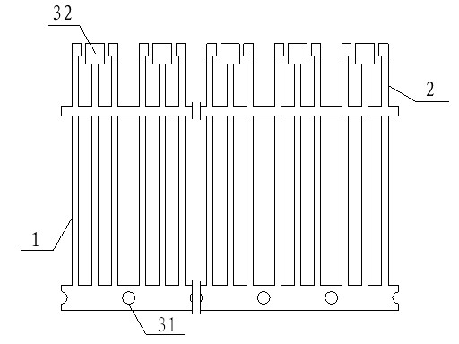
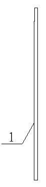
[0019] figure 1 , figure 2 The encapsulation box of the TO92S type shown includes a lead frame 1, pins 2, pads 32, and positioning holes 31. A pad 32 is installed in the empty circle on the small island at the head of the lead frame 1, and the pad 32 is used below the pad 32. The metal lead is connected to the pin 2. On the lead frame 1, the positioning holes 31 and the pads 32 are 60 and 35 in a single row respectively. The thickness of the lead frame 1 is 0.34 mm and the width is 17.3 mm. Increasing the number of positioning holes and the number of pads can improve productivity in terms of production efficiency.

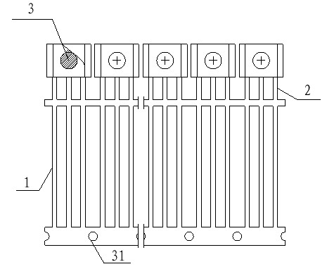
[0020] image 3 , Figure 4 After the TO92S model shown is added to the wafer 3 and plastic-encapsulated, the sealing shell 4 on the packaging box is sealed with a sealing shell 4 outside the entire island at the head of the lead frame 1. The corresponding matching mold adopts a mold of 1480 pieces, and the mold colloid flow channel The effect of using a narr...


PUM


Abstract

The invention relates to a TO92S packaging box and a matched die. The TO92S packaging box comprises a lead frame, pins, connecting pads, locating holes and a seal shell, wherein the connecting pads are arranged in an empty loop arranged on an islet on the head of the lead frame; the lower parts of the connecting pads are connected with the pins through metal leads; the outside of the whole islet is sealed by the seal shell; on the lead frame, the quantities of the locating holes and the connecting pads are respectively 60 and 35 in a single row; the lead frame is 0.34mm thick and 17.3mm wide; the seal shell is a trapezoid of which the middle is provided with a concave circle; and the correspondingly matched TO92S packaging die has 1480 molds, and the die colloid flow passage adopts a narrow type. The invention improves the packaging frame and the corresponding die, and perfects the use of equipment and raw materials in production, so that the equipment can operate better, faster and more precisely, and produce more products under the condition of the same quantity.

Description

technical field [0001] The invention relates to a TO92S type semiconductor package, in particular to an improved TO92S type package box and a supporting mold. Background technique [0002] Semiconductor packaging refers to the process of processing the wafers that have passed the test to obtain independent chips according to the functional requirements of the product model. The packaging of semiconductor chips is to paste the cut wafers on the small island of the lead frame with glue, and then use ultra-fine metal wires. The wiring pads of the chip are connected to the corresponding pins of the substrate, and then the independent chip is sealed and protected with a sealed casing. The package box of the semiconductor package of the model TO92S adopts a single row of 50 pieces, mainly 25 pieces, and the thickness is 0.38 mm and a width of 23.8mm, and the corresponding matching mold adopts a structure with a mold size of 1200 pieces. In this way, the use of raw materials and pr...

Claims


Application Information

Patent Timeline
Patent Type & Authority Applications(China)
IPC IPC(8): H01L23/495H01L23/31H01L23/04H01L21/56
CPCH01L2924/0002H01L2924/00
Inventor 周志刚
Owner WUJIANG SONGLING TOWN MINGBO PRECISION MACHINERY FACTORY
Why Eureka
Eureka Blog
Learn More