Light emitting device, illumination apparatus and display apparatus

A technology of light-emitting devices and light-emitting layers, which is applied in the fields of display equipment and lighting equipment, and can solve problems such as efficiency attenuation

Inactive Publication Date: 2012-09-19
SONY CORP
View PDF15 Cites 4 Cited by
  • Summary
  • Abstract
  • Description
  • Claims
  • Application Information

AI Technical Summary

Problems solved by technology

In this case, however, the effic

Method used


Image

  • Light emitting device, illumination apparatus and display apparatus
  • Light emitting device, illumination apparatus and display apparatus
  • Light emitting device, illumination apparatus and display apparatus

Examples


no. 1 approach

[0165] 1. First Embodiment (Organic EL Device)

[0166] 2. Second Embodiment (Organic EL Device)

no. 3 approach

[0167] 3. Third Embodiment (Organic EL Device)

[0168] 4. Fourth Embodiment (Organic EL Lighting Equipment)

[0169]5. Fifth Embodiment (Organic EL Display Device)

[0170] 1. First Embodiment (Organic EL Device)

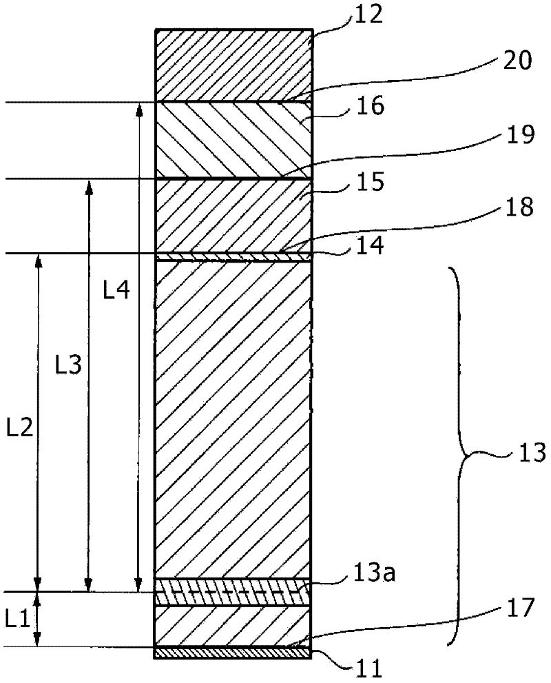
[0171] figure 1 is a cross-sectional view of the organic EL device according to the first embodiment.

[0172] Such as figure 1 As shown, in this organic EL device, the organic layer 13 is sandwiched between the first electrode 11 and the second electrode 12, serving as an organic layer including a light emitting layer 13a emitting monochromatic light at one position. The luminescent center of the luminescent layer 13a is represented by symbol O. The organic layer 13 includes portions above and below the light emitting layer 13a. Each of these portions above and below the light-emitting layer 13a includes layers such as a hole injection layer, a hole transfer layer, an electron transfer layer, and an electron injection layer as necessary, as in conventionally...

no. 1 example

[0220] The first example is an example of the first embodiment.

[0221] Figure 13 is a sectional view showing the organic EL device according to the first embodiment. The top surface light emitting organic EL device is a top surface light emitting type organic EL device. Such as Figure 13 As shown, the organic EL device is constructed by forming a laminate on a substrate 21 serving as the lowermost layer. The laminate is formed by sequentially forming a first electrode 11 , an organic layer 13 , a metal layer 14 , a transparent layer 15 , a transparent layer 16 , and a second electrode 12 in an upward direction. Then, a passivation film 22 is provided on the second electrode 12 . The organic layer 13 includes a light emitting layer 13a.

[0222] The substrate 21 is generally a transparent glass substrate or a semiconductor substrate such as a silicon substrate. The substrate 21 may also be configured as a flexible substrate.

[0223] The first electrode 11 serves as ...


PUM

PropertyMeasurementUnit
Thicknessaaaaaaaaaa
Thicknessaaaaaaaaaa
Thicknessaaaaaaaaaa

Abstract

Disclosed herein are a light emitting device, an illumination apparatus and a display apparatus, the light emitting device including: an organic layer sandwiched between a first electrode and a second electrode to serve as an organic layer including a light emitting layer for emitting monochromatic light at one location; a first light reflection boundary face provided on a side close to the first electrode to serve as a boundary face for reflecting light emitted from the light emitting layer so as to radiate the reflected light from a side close to the second electrode; and a second light reflection boundary face, a third light reflection boundary face and a fourth light reflection boundary face which are sequentially provided at positions separated away from each other in a direction from the first electrode to the second electrode on the side close to the second electrode.

Description

technical field [0001] The present invention relates to a light emitting device, a lighting device using the light emitting device, and a display device using the light emitting device. More specifically, the present technology relates to a light emitting device using electroluminescence of an organic material, a lighting device using the light emitting device, and a display device using the light emitting device. Background technique [0002] As a light-emitting device capable of emitting light with high luminance when driven at a low DC (direct current) voltage, a light-emitting device using electroluminescence of an organic material has attracted much attention, and such light-emitting devices have been extensively and intensively studied. In the following description, a light emitting device using electroluminescence of an organic material is referred to as an organic EL device. An organic EL device has a structure in which an organic layer is sandwiched between a light...

Claims


Application Information

Patent Timeline
IPC IPC(8): H01L51/52F21K99/00H01L27/32
CPCH01L27/3244H01L51/5265H01L2251/5361H10K59/12H10K50/852H10K50/805H10K50/856
Inventor 福田俊广
Owner SONY CORP
Why Eureka
Try Eureka