Wiring method of memory device

A wiring method and equipment technology, applied in the computer field, can solve problems such as small motherboard area, short distance between memory controller and memory device, and increased production cost of printed circuit board (PCB), so as to reduce the number of stacked layers and improve design Efficiency and production cost savings

Active Publication Date: 2012-09-26
江苏航天龙梦信息技术有限公司
View PDF4 Cites 8 Cited by
  • Summary
  • Abstract
  • Description
  • Claims
  • Application Information

AI Technical Summary

Problems solved by technology

It can solve the situation that the motherboard area is small, or the distance between the memory controller and the memory device is too close, etc., forcing all signal lines in the same data group to be routed on the same layer will increase the production of printed circuit boards (PCBs) cost problem

Method used


Image

  • Wiring method of memory device
  • Wiring method of memory device
  • Wiring method of memory device

Examples


Embodiment Construction

[0038] The preferred embodiments of the present invention will be described in detail below in conjunction with the accompanying drawings, so that the advantages and features of the present invention can be more easily understood by those skilled in the art, so as to define the protection scope of the present invention more clearly.

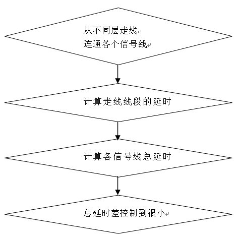
[0039] see figure 1 , the embodiment of the present invention includes:

[0040] A wiring method of a memory device of the present invention, the specific steps include:

[0041] (1) Connect each signal line of the same data group between the memory controller and the memory device, and the wiring can be routed from multiple wiring layers of the printed circuit board (PCB) at the same time.

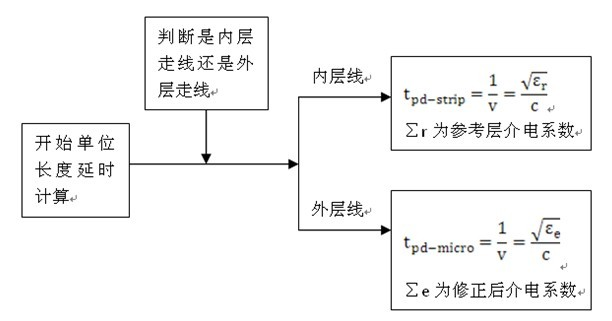
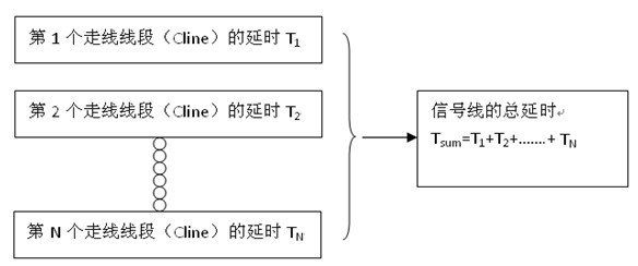
[0042] (2) According to the delay T of the line segment (Cline) per unit length D The calculation method calculates the delay of all the line segments (Cline) of each signal line respectively. Delay (T i ) is equal to the delay (T D ) times the length (...


PUM


Abstract

The invention discloses a wiring method of a memory device, comprising the steps of communicating signal wires in a same data array between a memory controller and the memory device; performing wiring from a plurality of wiring layers of a printed-circuit board; computing delay of all wiring sections of all signal wires respectively; computing total delay TSUM of all signal wires in the same data array; and controlling absolute value of difference value of the total delay of all signal wires to be in the limit range by regulating surface wire length or inner wire length of each signal wire. The wiring method of the memory device has the advantages that in the printed-circuit board, the wiring method is not limited by the fact that the signal wires in the same data array must be wired in the same layer. According to the wiring method, the design efficiency of the printed-circuit board can be improved, and the distance between the memory control chip and the memory device is closer or the lamination number of the printed-circuit board is reduced, so that the manufacturing cost of the printed-circuit board is lowered.

Description

technical field [0001] The invention relates to a memory wiring method in the field of computers, in particular to a memory part wiring method in printed circuit board (PCB) design. Background technique [0002] Usually, in the layout guide of the memory controller, in the routing design of the memory part of the printed circuit board (PCB), the signal lines of the same data group must be routed on the same layer, and the number of vias should be kept the same. That is to say, even if the signal lines of the same data group need to jump layers, they must be jumped at the same time, so as to ensure that the line segments (Clines) of each signal line are of the same length in the passing wiring layers, and the same The data sets have the same number of punched holes for the signal lines. [0003] Whether it is double data rate 1 (DDR1), double data rate 2 (DDR2), or double data rate 3 (DDR3), this requirement is usually included in the layout guide of the memory controller. ...

Claims


Application Information

Patent Timeline
Patent Type & Authority Applications(China)
IPC IPC(8): G06F17/50
Inventor 吴少刚张福新周国强张斌徐锋崔太有
Owner 江苏航天龙梦信息技术有限公司
Why Eureka
Try Eureka