
Pixel circuit structure and method for driving pixel circuit structure

A pixel circuit and drive transistor technology, applied in the field of OLED, can solve the problems of panel brightness difference, poor brightness uniformity, different OLED drive current, etc., and achieve the effect of stable drive current and improved uniformity

Active Publication Date: 2012-09-26
BOE TECH GRP CO LTD +1
View PDF4 Cites 17 Cited by
  • Summary
  • Abstract
  • Description
  • Claims
  • Application Information

AI Technical Summary

Problems solved by technology

[0004] Due to the immaturity of the LTPS (low temperature polysilicon) process, at the same time V th There is also drift, even with the same process parameters, the V of TFTs produced in different positions th There is also a large difference, which leads to different driving currents of OLEDs under the same gray scale voltage, so the brightness of different positions of the panel under this driving scheme will be different, and the brightness uniformity is poor

Method used


Image

  • Pixel circuit structure and method for driving pixel circuit structure
  • Pixel circuit structure and method for driving pixel circuit structure
  • Pixel circuit structure and method for driving pixel circuit structure

Examples


Embodiment Construction

[0041] In order to make the technical problems, technical solutions and advantages to be solved by the embodiments of the present invention clearer, the following will describe in detail with reference to the drawings and specific embodiments.

[0042] The embodiments of the present invention aim at the problem of poor panel luminance uniformity in the prior art, and provide a pixel circuit structure and a method for driving the pixel circuit structure, which can realize uniform current, thereby improving the uniformity of panel luminance.

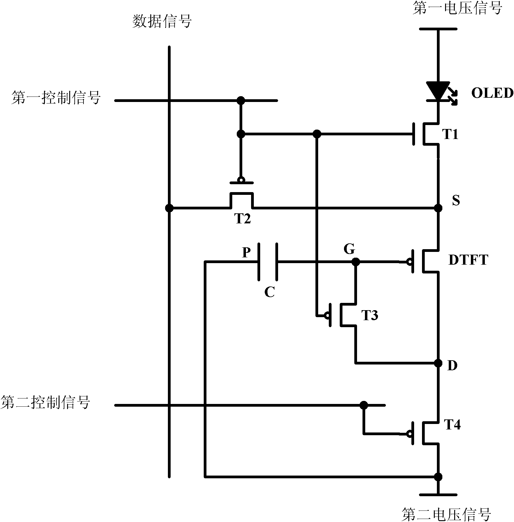
[0043] An embodiment of the present invention provides a pixel circuit structure, including a light-emitting device connected in series between a first voltage signal terminal and a second voltage signal terminal and a driving transistor for driving the light-emitting device. Capacitance between the gates of the driving transistor, the source of the driving transistor is used to receive the data signal and the first voltage signal; the pixe...


PUM


Abstract

The invention provides a pixel circuit structure and a method for driving the pixel circuit structure, which relate to the field of organic light-emitting diodes. The pixel circuit structure comprises a first switch transistor and a fourth transistor, wherein the first switch transistor is used for responding to a first control signal received by the grid of the first switch transistor, and disconnecting / connecting a first voltage signal terminal from / with the source of a drive transistor; the fourth transistor is used for responding to a second control signal received by the grid of the fourth transistor, and disconnecting / connecting the drain of the drive transistor from / with a second voltage signal terminal; when the drain and grid of the drive transistor are connected, the drain of the drive transistor and the second voltage signal terminal are disconnected, so that the drive transistor begins to discharge until the voltage between the source and grid of the drive transistor is equal to a threshold voltage. According to the embodiment of the invention, the stability of a driving current is realized, and the brightness uniformity of a panel is improved. The pixel circuit structure and method for driving the pixel circuit structure disclosed by the invention are suitable to be used in organic light-emitting diode systems.

Description

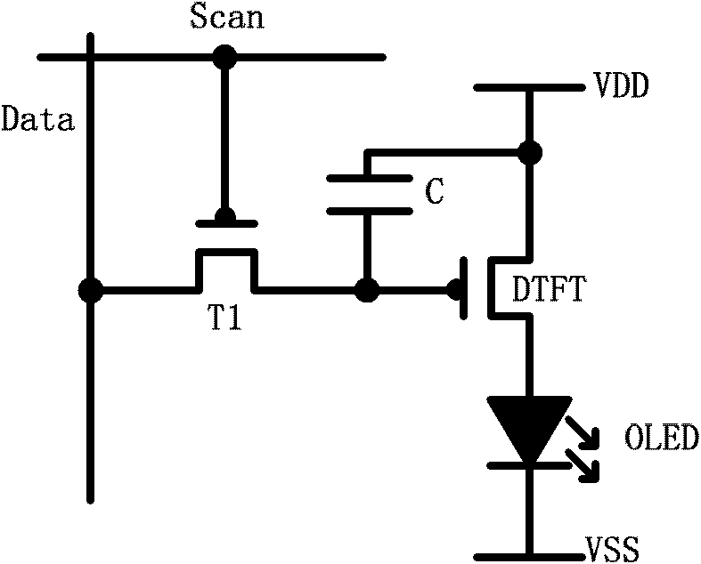
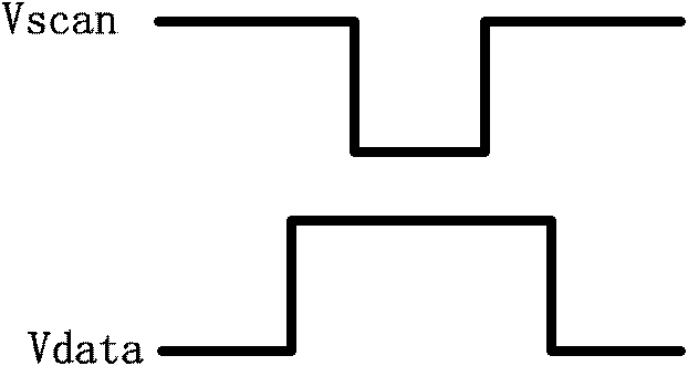
technical field [0001] The present invention relates to the field of OLED (Organic Light-Emitting Diode, organic light-emitting diode), in particular to a pixel circuit structure and a method for driving the pixel circuit structure. Background technique [0002] AMOLED (Active Matrix / Organic Light Emitting Diode, active matrix organic light emitting diode panel) can emit light is driven by the current generated by driving TFT (Thin Film Transistor, thin film field effect transistor) in saturation state, because the same input When the grayscale voltage is used, different threshold voltages will generate different driving currents, resulting in inconsistency of the currents. [0003] The traditional 2T1C circuit such as figure 1 As shown, the circuit contains only two TFTs, T1 is used as a switch, and DTFT (driver transistor) is used for pixel driving. The circuit operation is also relatively simple, the timing diagram is as follows figure 2 As shown, when the scanning le...

Claims


Application Information

Patent Timeline
Patent Type & Authority Applications(China)
IPC IPC(8): G09G3/32G09G3/3225
Inventor 青海刚祁小敬高永益
Owner BOE TECH GRP CO LTD
Learn More