
Address jump output device and method

A technology of address jumping and output device, applied in information storage, static memory, digital memory information and other directions, can solve problems such as easy conflict and error, complex implementation, troublesome, etc., to reduce resource consumption and error probability, and reduce overhead. Effect

Inactive Publication Date: 2012-10-03
TECHTOTOP MICROELECTRONICS
View PDF7 Cites 5 Cited by
  • Summary
  • Abstract
  • Description
  • Claims
  • Application Information

AI Technical Summary

Problems solved by technology

But in this way, each part needs to make different counting condition judgments, which is very troublesome and prone to conflicts and errors
For example, the address generation circuit mentioned in the CN102160032A patent, which sets the block size and jump size, is essentially based on a judgment on the jump condition, and this approach does not reduce much complexity.
Another example is the "effective address = (segment + displacement) + base address + (change * ratio)" mentioned in the CN101027633A patent. occasion

Method used


Image

  • Address jump output device and method
  • Address jump output device and method
  • Address jump output device and method

Examples


Embodiment Construction

[0016] In order to make the objectives, technical solutions and advantages of the present invention clearer, the following further describes the present invention in detail with reference to the accompanying drawings and embodiments. It should be understood that the specific embodiments described herein are only used to explain the present invention, but not to limit the present invention.

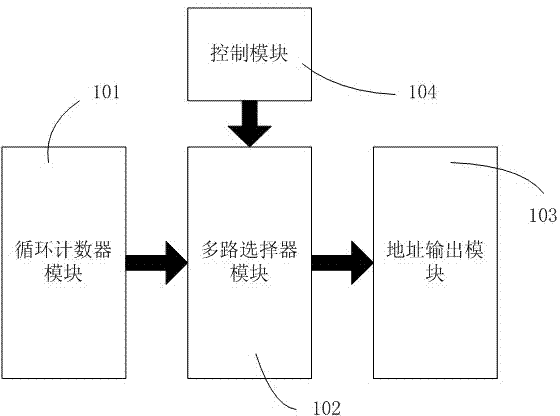
[0017] Attached figure 1 It is a schematic structural diagram of an embodiment of the present invention. In this embodiment, the device is divided into 4 parts:

[0018] The first part, 101, is a cycle counter module. The counter module can contain at least one register as needed. The counter will continuously perform "+1" counting operations driven by the system clock. The count value is added from 0 to the upper limit of the value that the register can represent, and then returns to 0 to restart the accumulation.

[0019] The second part, 102, is a multiplexer module, the module is a multiple...


PUM


Abstract

The invention discloses an address jump output device. The device comprises a cycle counter module, a multiplexer module, a control module and an address output module; wherein the cycle counter module outputs a count value to the multiplexer module; the control module outputs a control command to the multiplexer module so as to control the operation of the count value, and finally, the operation result of the multiplexer module is output to the address output module. With the adoption of the technical scheme, the design cost can be effectively reduced, and the resource consumption and error probability of the jump circuit are reduced.

Description

Technical field [0001] The invention relates to an address jump output device and method. Background technique [0002] At present, in chip circuit design, address jump is a frequently encountered problem. Many times, different address jump methods are required in different parts of the circuit. For example, the first part needs to jump to addresses according to 0,64,128,192,1,65,129,193..., while the second part becomes according to 0,16,32, 48, 1, 17, 33, 49... Jump like this. In the traditional solution, different parts of the circuit will be counted in different ways to achieve the required jump effect. But in this way, each part needs to make different counting condition judgments, which is very troublesome and easy to conflict and make mistakes. For example, the address generation circuit mentioned in the CN102160032A patent, which sets the block size and skip size, is essentially based on a judgment of the skip condition, and this approach does not reduce the complexity...

Claims


Application Information

Patent Timeline
Patent Type & Authority Applications(China)
IPC IPC(8): G11C8/04
Inventor 何毅华
Owner TECHTOTOP MICROELECTRONICS
Learn More