
Light-emitting diode and its manufacturing method

A technology for light-emitting diodes and a manufacturing method, which is applied to electrical components, electrical solid-state devices, circuits, etc., can solve problems such as peeling off of phosphor powder layers, and achieve the effects of reducing investment in production equipment, increasing design freedom, and reducing process costs.

Active Publication Date: 2015-11-25
LIGHTIZER KOREA
View PDF10 Cites 0 Cited by
  • Summary
  • Abstract
  • Description
  • Claims
  • Application Information

AI Technical Summary

Problems solved by technology

However, the above-mentioned phosphor powder layer is directly coated on the above-mentioned semiconductor light-emitting device, and there is a problem that the phosphor powder layer peels off.

Method used


Image

  • Light-emitting diode and its manufacturing method
  • Light-emitting diode and its manufacturing method
  • Light-emitting diode and its manufacturing method

Examples


Embodiment Construction

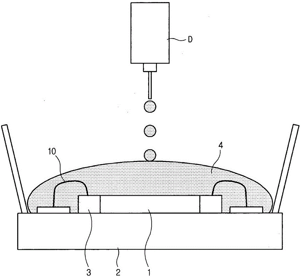
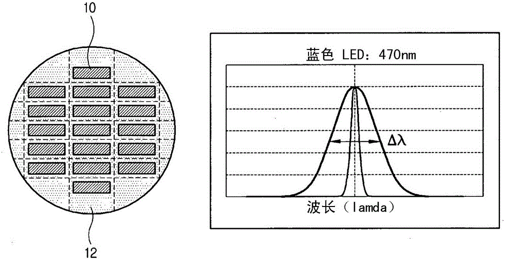
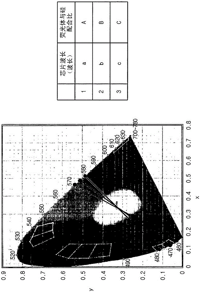
[0060] As described above, the present invention relates to a light emitting diode capable of outputting light of a desired wavelength by coating a phosphor / silicon complex layer and a method of manufacturing the same. In more detail, it is assumed that the wavelength of light emitted from a light emitting diode (LED) (assumed blue LED, ultraviolet LED) is measured at the wafer level. Based on the above wavelength measurement results, a conformal coating is applied to the above LED. The above-mentioned conformal coating has a phosphor compounding ratio based on the above-mentioned wavelength. In addition, the phosphor compounding ratio includes at least one of yellow, green, or red. Therefore, the light output from the above-mentioned LED is converted into white light using a conformal coating. In the embodiment of the present invention, these steps are performed at the wafer level, which can achieve better uniformity and inertia.

[0061] On the other hand, in the MOCVD (meta...


PUM


Abstract

The present invention relates to a light emitting diode (LED) that enhances productivity and a method for manufacturing same. The disclosed LED comprises: a light emitting semiconductor chip which is provided with a n-type semiconductor layer, an active layer, and a p-type semiconductor layer; a fluorescent material layer which has a luminescence mixing ratio that is based on the wavelength of the emitted light from the light emitting semiconductor chip so that the light emitted from the light emitting semiconductor chip is converted to a desired intensity, and which is coated on the top surface of the light emitting semiconductor chip; and a connecting layer which is placed between the fluorescent material layer and the light emitting semiconductor chip and connects the fluorescent material layer to the light emitting semiconductor chip.

Description

Technical field [0001] The present invention relates to a light emitting diode and a manufacturing method thereof, in particular to a light emitting diode and a manufacturing method thereof capable of improving productivity. Background technique [0002] As a high-efficiency product, the use of light-emitting diodes (LightEmittingDiode: LED) is increasing, and research and development on it continue. In this respect, it is difficult to reflect the white light output from the light emitting diode. In the past, many new methods for reflecting white light have been tried [0003] However, these many approaches are not performed at the wafer level, but at the chip level. This approach causes chip waste. [0004] Moreover, no existing method can change the ratio of phosphors (fluorescent substances) based on fundamental measurement results such as the wavelength of output light. [0005] Therefore, light-emitting diodes and manufacturing methods based on new approaches are required. [0...

Claims


Application Information

Patent Timeline
Patent Type & Authority Patents(China)
IPC IPC(8): H01L33/50
CPCH01L33/50H01L33/44H01L2224/48091H01L2933/0041H01L27/153H01L2924/00014H01L33/48
Inventor 赵炳求
Owner LIGHTIZER KOREA
Learn More