Method of driving non-volatile logic circuit and non-volatile logic circuit

A logic circuit, non-volatile technology, applied to logic circuits using basic logic circuit components, logic circuits using specific components, logic circuits with logic functions, etc., can solve problems such as short circuits

Inactive Publication Date: 2015-12-02
PANASONIC CORP
View PDF5 Cites 0 Cited by
  • Summary
  • Abstract
  • Description
  • Claims
  • Application Information

AI Technical Summary

Problems solved by technology

As a result, the conduction state between the semiconductor layer 14 and the second electrode 15 becomes a short circuit again.

Method used


Image

  • Method of driving non-volatile logic circuit and non-volatile logic circuit
  • Method of driving non-volatile logic circuit and non-volatile logic circuit
  • Method of driving non-volatile logic circuit and non-volatile logic circuit

Examples


Embodiment approach 1

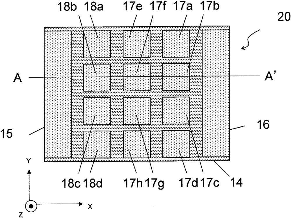
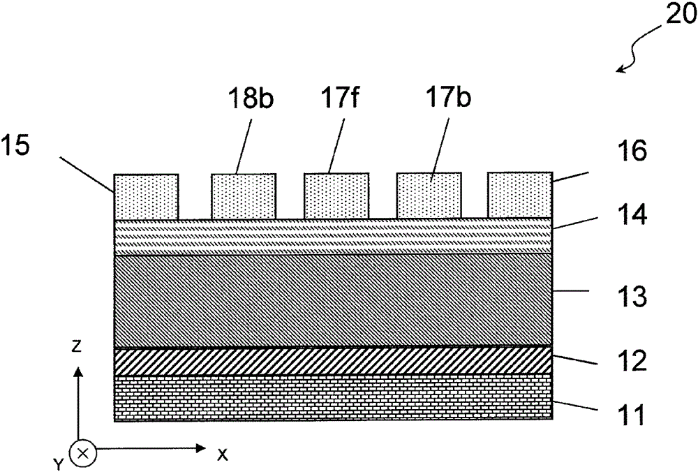
[0100] (Structure of the nonvolatile logic circuit 20)

[0101] Figure 1A A plan view of the nonvolatile logic circuit 20 according to Embodiment 1 is shown. Figure 1B express Figure 1A The cross-sectional view of A-A' in.

[0102] like Figure 1B As shown, a control electrode 12 , a ferroelectric film 13 , a semiconductor film 14 , and electrode groups 15 to 18 are sequentially stacked on a substrate 11 .

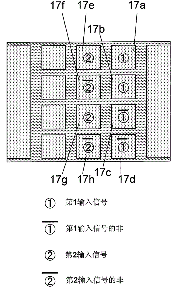
[0103] The electrode group has a power supply electrode 15, an output electrode 16, first to eighth input electrodes 17a to 17h, and first to fourth logic setting electrodes 18a to 18d.

[0104] like Figure 1A and Figure 1B As shown, the X direction, the Y direction, and the Z direction are the longitudinal direction, the direction perpendicular to the longitudinal direction, and the stacking direction of the ferroelectric film (13), respectively.

[0105] Along the X direction, the first to eighth input electrodes 17 a to 17 h and the first to fourth logic set...

Embodiment 1

[0199] (1) On the silicon substrate 11 having a surface covered with a silicon oxide film, a titanium film having a thickness of 5 nm and a platinum film having a thickness of 30 nm were sequentially formed using an electron gun evaporation method. Furthermore, SrRuO with a thickness of 10 nm was formed by pulsed laser deposition 3 (hereinafter referred to as SRO) film. In this manner, control electrode 12 is formed on silicon substrate 11 .

[0200] (2) The substrate was heated to 700°C. In the PLD cavity, a Pb(Zr,Ti)O 3 constituted ferroelectric film 13.

[0201] (3) The temperature of the substrate was set to 400° C., and a semiconductor film 14 made of ZnO was formed to have a thickness of 30 nm in the PLD chamber.

[0202] (4) On the semiconductor film 14, a resist pattern is formed by photolithography. Thereafter, portions of the semiconductor film 14 not covered with the resist are removed by etching using nitric acid.

[0203] (5) On the semiconductor film 14, a ...


PUM


Abstract

A nonvolatile logic circuit includes logic configuration electrodes and input electrodes. The nonvolatile logic circuit is programmable to any one of the logics between the input signals selected from logical conjunction (AND), logical disjunction (OR), logical non-conjunction (NAND), logical non-disjunction (NOR), and logical exclusive disjunction (XOR) by changing applied voltages to the logic configuration electrodes.

Description

technical field [0001] The present invention relates to methods of driving non-volatile logic circuits. Background technique [0002] Figure 10 ~ Fig. 14 is Fig. 1 of Patent Document 1 ~ Figure 5 . [0003] like Figure 10 As shown, the semiconductor storage device 10 of the present invention has a laminated film composed of a ferroelectric layer 13 and a semiconductor layer 14, the first electrode 12 is formed on the ferroelectric layer 13 side of the laminated film, and the semiconductor layer 14 of the laminated film is formed. A plurality of second electrodes 15a to 15c are formed on the layer 14 side. In addition, these layers are formed on the substrate 11 . [0004] Figure 11A and Figure 11B is a diagram showing the initial state of the semiconductor memory device, Figure 11A is a cross-sectional stereogram, Figure 11B Indicates the equivalent circuit diagram. [0005] For example, when an n-type semiconductor is used for the semiconductor layer 14, in t...

Claims


Application Information

Patent Timeline
Patent Type & Authority Patents(China)
IPC IPC(8): H03K19/20
CPCH03K19/173
Inventor 金子幸广
Owner PANASONIC CORP
Why Eureka
Try Eureka