Proximity contact scan exposure device and method

A technology of scanning exposure and exposure device, applied in the field of lithography, can solve the problems of irreplaceable Aligner and high cost

CN102736421BActive Publication Date: 2015-06-17SHANGHAI MICRO ELECTRONICS EQUIP (GRP) CO LTD
7 Cites 0 Cited by

Patent Information

Authority / Receiving Office
CN · China
Patent Type
Patents(China)
Current Assignee / Owner
Publication Date
2015-06-17

Smart Images

  • Figure 1
    Figure 1
  • Figure 2
    Figure 2
  • Figure 3
    Figure 3
Patent Text Reader

Abstract

The invention discloses a proximity contact scan exposure device which successively comprises the following parts along the optical propagation direction: an illumination system which is used for outputting parallel lights; a mask which is irradiated by the parallel lights to generate emergent light output; a substrate which is positioned below the mask and is irradiated by the emergent lights emitted from the mask; and a working table which supports the mask and the substrate. When the scan exposure device is in use, the mask and the substrate synchronously move with the working table. In comparison with a traditional aligned mask aligner, although the yield of the device provided by the invention is a little lower, dose uniformity is raised such that linewidth uniformity (CDU) is improved. In comparison with a traditional projection type mask aligner, although precision of the device provided by the invention is not such high, projection lens is not required so as to reduce the cost.
Need to check novelty before this filing date? Find Prior Art

Description

technical field

[0001] The invention relates to the field of photolithography, in particular to a near-contact scanning exposure device and method for photolithography devices. Background technique

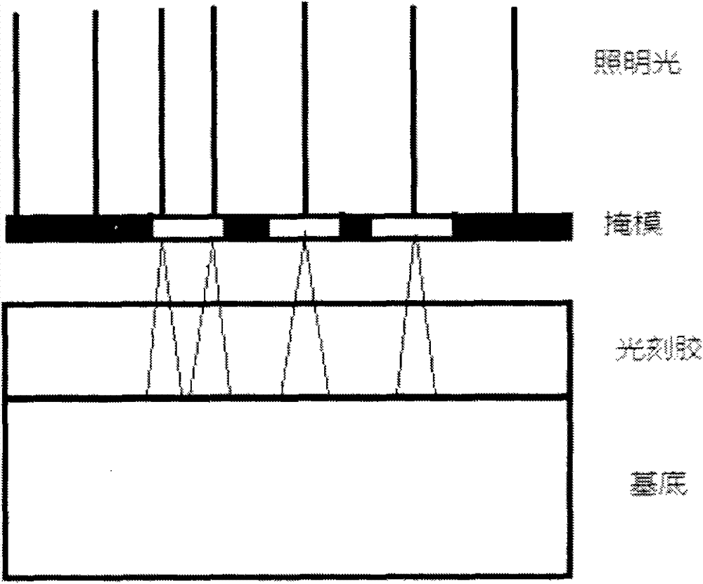
[0002] The most commonly used lithography machine for exposure above 1um is mask alignment MaskAligner. MaskAligner is a common approach to contact exposure method. Such an exposure method is described. With the upgrading of the industry, the size of the substrate is getting bigger and bigger, and the lighting area is also getting bigger and bigger. In this case, as figure 1 As shown, when using Mask Aligner exposure, the illumination uniformity error causes the photoresist dose error, which seriously affects the line width uniformity of the substrate.

[0003] The IC industry generally uses a projection lithography machine for exposure. This method has higher exposure precision and better CD uniformity. However, the cost of projection lithography is much higher than that o...

Examples

Embodiment Construction

[0032] In the following, preferred embodiments according to the present invention will be described in detail with reference to the accompanying drawings. For the convenience of describing and highlighting the present invention, relevant components existing in the prior art are omitted from the drawings, and the description of these known components will be omitted.

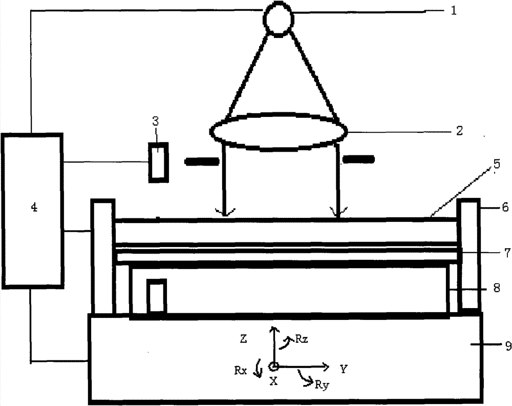
[0033] figure 2 Shown is a schematic structural view of an embodiment of the exposure apparatus according to the present invention. The exposure device includes a light source 1, an optical path system 2, a workpiece table 9 (including a suction cup 8 and a clamp 6), an alignment system 3, a control system 4, and the like. The light source 1 can be a mercury lamp, which provides uniform parallel light illumination to the mask 5 through the optical path system 2, which has a shutter and a variable slit. The mask 5 is mounted on the workpiece table fixture 6, which can fine-tune the position of the mask. The ma...