Chip taking and placing device

A pick-and-place device and chip technology, which is applied in the direction of electrical components, semiconductor/solid-state device manufacturing, circuits, etc., can solve the problems of limiting production efficiency and low operating efficiency, and achieve the effect of improving production efficiency and improving efficiency

Inactive Publication Date: 2012-10-24
EVERLIGHT ELECTRONICS (CHINA) CO LTD +1
View PDF4 Cites 4 Cited by
  • Summary
  • Abstract
  • Description
  • Claims
  • Application Information

AI Technical Summary

Problems solved by technology

However, such a chip pick-and-place device has low operating efficiency, which limits the overall production efficiency

Method used


Image

  • Chip taking and placing device
  • Chip taking and placing device
  • Chip taking and placing device

Examples


Embodiment Construction

[0035] The specific embodiments of the invention will be described below with reference to the accompanying drawings. The descriptions of the specific embodiments are only for explaining the invention and are not intended to limit the invention.

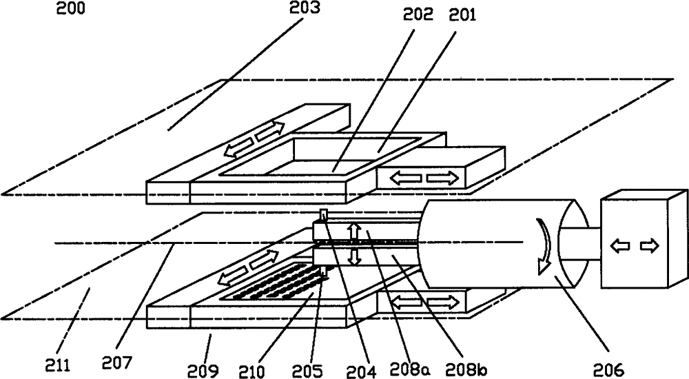
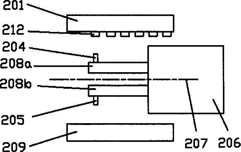
[0036] figure 2 It is a schematic structural diagram of the first embodiment of the chip pick-and-place device of the present invention. Please refer to figure 2 As shown, the chip pick-and-place device 200 mainly includes: a chip storage area 201, a chip placement area 209, two suction nozzles 204 and 205, a rotating shaft 206, and two telescopic rods 208a and 208b connecting the two suction nozzles and the rotating shaft. The chip storage area 201 has a first working plane 203, and the first working plane 203 is a working plane of the chip storage area 201 for storing the chip storage disk 202 of the chip to be sucked. The chip placement area 209 has a second working plane 211, and the second working plane 211 is the working plane o...


PUM


Abstract

The invention provides a chip taking and placing device which can be used for technologies including a preparation technology of light-emitting diodes and the like which require chip movement. The chip taking and placing device comprises a chip storage area, a chip placing area, a rotating shaft, a first sucking nozzle and a second sucking nozzle, wherein the first sucking nozzle and the second sucking nozzle are arranged on the rotating shaft, and the rotating shaft rotates to drive the first sucking nozzle and the second sucking nozzle to place chips from the chip storage area to the chip placing area. The chip taking and placing device is characterized in that the first sucking nozzle and the second sucking nozzle are in even symmetry around the axis of the rotating shaft and on the same plane perpendicular to the axis of the rotating shaft and are distributed corresponding to the chip storage area and the chip placing area. The chip taking and placing device can perform sucking-taking and placing simultaneously, thereby effectively improving the overall production efficiency.

Description

Technical field [0001] The invention relates to a pick-and-place device, in particular to a pick-and-place device for light-emitting diode chips. Background technique [0002] Light-emitting diodes are known as the green lighting products of the 21st century. They have attracted much attention for their advantages of low working voltage, low power consumption, high luminous efficiency, and long life. An important component in the light-emitting diode structure is the chip. It is precisely because of the chip that the light-emitting diode will emit light. When making light-emitting diodes, the wafer is cut into individual chips, and the chip is fixed on the support of the light-emitting diode using a die bonding process. Because the chip is small and easily broken, it is difficult to manually move the chip during the die bonding process. [0003] In order to solve the above problems, a special chip pick-and-place device is generally used to pick up the chip and place it in a pred...

Claims


Application Information

Patent Timeline
Patent Type & Authority Applications(China)
IPC IPC(8): H01L21/00H01L21/683H01L33/00
Inventor 叶寅夫林文琪潘科豪
Owner EVERLIGHT ELECTRONICS (CHINA) CO LTD
Why Eureka
Try Eureka