Device for obtaining a multicrystalline semiconductor material, in particular silicon, and method for controlling the temperature therein

A semiconductor and polysilicon technology, applied in the field of polysilicon semiconductor materials, can solve problems such as high energy consumption and long time

Inactive Publication Date: 2012-10-24
赛亚特股份有限公司
View PDF2 Cites 4 Cited by
  • Summary
  • Abstract
  • Description
  • Claims
  • Application Information

AI Technical Summary

Problems solved by technology

In addition, the melting step of the solid semiconducting material to be refined requires a long time and high energy consumption

Method used


Image

  • Device for obtaining a multicrystalline semiconductor material, in particular silicon, and method for controlling the temperature therein
  • Device for obtaining a multicrystalline semiconductor material, in particular silicon, and method for controlling the temperature therein
  • Device for obtaining a multicrystalline semiconductor material, in particular silicon, and method for controlling the temperature therein

Examples


Embodiment Construction

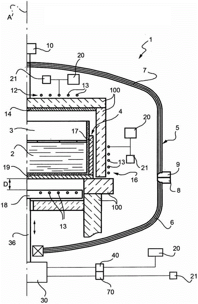
[0020] refer to figure 1 and 2 , an apparatus for melting and subsequent directional solidification of semiconductor material 2 , in particular for obtaining polysilicon of “solar purity”, is indicated overall by 1 .

[0021] Said device 1 comprises: at least one crucible 3 for semiconductor material 2, preferably made of quartz or ceramic material, removably housed in a cup-shaped graphite container 4; and a fluid-tight enclosure 5, inside which The graphite container 4, fluid-tight cover 5 comprises a cup-shaped bottom half-shell 6 and top half-shell 7; said bottom half-shell 6 and top half-shell 7 are preferably made of steel, usually with their concave faces facing each other connected one above the other ( figure 1 ), and appropriate gaskets (not shown) are provided on each edge 8, 9 to butt together in a fluid-tight manner.

[0022] Said apparatus 1 further comprises means 10 for vertically removing the top half-shell 7 from the bottom half-shell 6 so that the cover 5...


PUM


Abstract

A device (1) for obtaining multicrystalline silicon, including: at least one crucible (3) made of quartz for the silicon, removably housed in a cup-shaped graphite container (4); a fluid- tight openable casing (5); a top induction coil (12), set facing, with interposition of a graphite plate (14), the crucible, a lateral induction coil (16), set around a side wall (17) of the graphite container, and a bottom induction coil (18), set facing a bottom wall (19) of the graphite container and vertically mobile for varying the distance (D) from the bottom wall; and first means (20) for a.c. electrical supply of the induction coils separately from one another, and second means (21) for supply of a coolant within respective hollow turns of the induction coils; the bottom induction coil includes four spiral windings (31-34), arranged alongside one another according to a chequered scheme in one and the same plane of lie, which is defined by an insulated supporting plate (35); electrical switching means (40) enable in use selective connection of the four windings (31-34) to one another according to different configurations.

Description

technical field [0001] The invention relates to an apparatus for obtaining polysilicon semiconductor material, in particular silicon, by melting the semiconductor material and subsequently directional solidifying it, and a method for obtaining better control over the temperature of said semiconductor material. Background technique [0002] There is an increasing demand for semiconductor materials, especially silicon, of high purity, known as "solar purity", which can be used to produce high-efficiency photovoltaic cells. [0003] To obtain such materials, they are first purified by conventional metallurgical processes and finally formed into ingots, from which the wafers required for the production of photovoltaic cells are cut out. The ingot is formed using the method known as "Directional Solidification System" (DSS), ie by melting semiconductor material in a crucible and then directional solidifying it, resulting in polysilicon. [0004] To obtain directional solidificat...

Claims


Application Information

Patent Timeline
Patent Type & Authority Applications(China)
IPC IPC(8): C30B11/00B22D27/04F27B14/14H05B6/36H05B6/44C30B29/06C30B35/00
CPCH05B6/362F27B14/14H05B6/367C30B29/06H05B6/24C30B35/00H05B6/44C30B11/003B22D27/045C30B11/00B22D27/04
Inventor 发布里奇奥·杜吉罗米歇尔·福尔赞达里奥·齐斯卡托马里奥力诺·切萨诺发布里奇奥·克里韦洛罗伯托·贝基尼
Owner 赛亚特股份有限公司
Why Eureka
Try Eureka