Light convergence device, manufacturing method thereof and solar battery system
A solar cell and concentrating device technology, applied in the field of light energy, can solve problems such as low reflectivity, reduced conversion efficiency, and large loss of light wave energy
- Summary
- Abstract
- Description
- Claims
- Application Information
AI Technical Summary
Problems solved by technology
Method used
Image
Examples
Embodiment 1
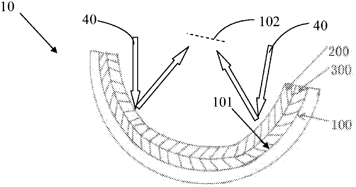
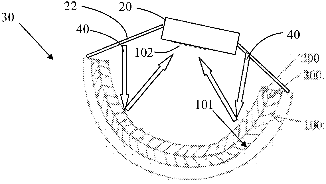
[0043] The structure of the light concentrating device of this embodiment is as follows: figure 1 As shown, wherein the concentrating substrate 100 adopts concave glass with a parabolic concave surface of rotation 101, and the photonic crystal layer 300 adopts polymer latex particles with a hard core-soft shell structure, and the particle diameter of the colloidal particles is about 500 nm. The photonic crystal layer 300 has a thickness of about 1000 nanometers, and the up-conversion material of the up-conversion layer 200 is Cs 3 Lu 2 Br 9 :Er 3+ , the thickness of the up-conversion layer 200 is about 0.1 μm.
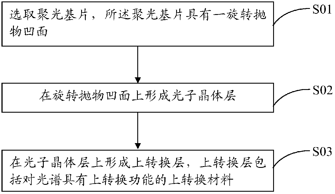
[0044] The specific manufacturing process of the light concentrating device of the above-mentioned embodiment is as follows:
[0045] (1) Prepare a piece of concave glass as the substrate, wash it and dry it for later use;
[0046] (2) According to the preparation method provided by the Chinese patent application number 200510011219.1, prepare an emulsion of monod...
Embodiment 2
[0049] The structure of the light concentrating device of this embodiment is as follows: figure 1 As shown, wherein, the concentrating substrate 100 is made of concave plexiglass with a parabolic concave surface of revolution 101, and the photonic crystal layer 300 is made of polymer latex particles with a hard core-soft shell structure, and the particle size of the particles is about 650nm. The thickness of the layer 300 is about 1300 nanometers, and the up-conversion material of the up-conversion layer 200 adopts CaS:Eu 3+ / Sm 3+ , the thickness of the up-conversion layer 200 is about 20 μm.
[0050] The specific manufacturing process of the light concentrating device of the above-mentioned embodiment is as follows:
[0051] (1) Prepare a piece of concave plexiglass as the substrate, wash it and dry it for later use;
[0052] (2) According to the preparation method provided by the Chinese patent application number 200510011219.1, prepare an emulsion of monodisperse polyme...
Embodiment 3
[0055] The structure of the light concentrating device of this embodiment is as follows: figure 1 As shown, wherein the concentrating substrate 100 is made of concave plastic with a parabolic concave surface of revolution 101, and the photonic crystal layer 300 is made of SiO 2 and TiO 2 , the thickness of the photonic crystal layer 300 is about 480 nanometers, and the up-conversion material of the up-conversion layer 200 adopts BaY 2 f 8 :Yb 3+ / Ho 3+ , the thickness of the up-conversion layer 200 is about 10 μm.
[0056] The specific manufacturing process of the light concentrating device of the above-mentioned embodiment is as follows:
[0057] (1) Prepare a piece of concave plastic as the substrate, wash it and dry it for use;
[0058] (2) According to the preparation method provided by the Chinese patent application number 200410018081, SiO is alternately grown on the substrate by ultra-high vacuum electron beam evaporation 2 and TiO 2 Thin film, 8 layers each, de...
PUM
| Property | Measurement | Unit |
|---|---|---|
| thickness | aaaaa | aaaaa |
| thickness | aaaaa | aaaaa |
| particle size | aaaaa | aaaaa |
Abstract
Description
Claims
Application Information
 - R&D
- Intellectual Property
- Life Sciences
- Materials
- Tech Scout
- Unparalleled Data Quality
- Higher Quality Content
- 60% Fewer Hallucinations
Browse by: Latest US Patents, China's latest patents, Technical Efficacy Thesaurus, Application Domain, Technology Topic, Popular Technical Reports.
© 2025 PatSnap. All rights reserved.Legal|Privacy policy|Modern Slavery Act Transparency Statement|Sitemap|About US| Contact US: help@patsnap.com


