
Systems and methods providing arrangements of vias

A chip and semiconductor technology, applied in the direction of semiconductor/solid-state device parts, semiconductor devices, electrical components, etc., can solve the problems of torque increase, affecting the mutual contact and alignment of ball grid arrays, etc.

Active Publication Date: 2012-11-14
QUALCOMM INC
View PDF5 Cites 0 Cited by
  • Summary
  • Abstract
  • Description
  • Claims
  • Application Information

AI Technical Summary

Problems solved by technology

During production, an underfill (not shown) may be added to the chip package 100 to provide mechanical support to the various components, but the stress around the periphery of the memory chip during production (before the underfill is added) can lead to impacts on the ball grid. Mutual Contact and Alignment Torque of Lattice Arrays 103, 106
As the amount of surface area of ​​the backside of the memory chip 101 not covered by the ball grid array 103 increases, the torque problem also increases.

Method used


Image

  • Systems and methods providing arrangements of vias
  • Systems and methods providing arrangements of vias
  • Systems and methods providing arrangements of vias

Examples


Embodiment Construction

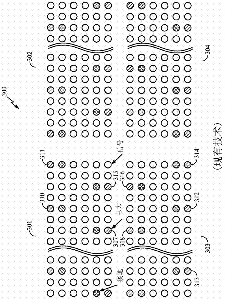
[0023] Figure 4 is an illustration of an exemplary system 400 adapted according to one embodiment. The system 400 includes a logic chip 402 and a memory chip 401 . The memory chip 401 includes contacts 422 , 423 and the logic chip 402 includes contacts 412 , 413 . For your convenience, Figure 4 Only four contacts 412, 413, 422, 423 are shown, but it is understood that various embodiments may include many more contacts arranged in an array. exist Figure 4 , the contacts are arranged in an array, the contacts being aligned to provide electrical contact between the logic chip 402 and the memory chip 401 . Specifically, the contacts 422 and 423 communicate with the redistribution layer 415 to access various memory cells (not shown) in the memory chip 401 . Likewise, contacts 412 and 413 communicate with logic circuits (not shown) and metal layer 418 via through-silicon vias (TSVs) 416 , 417 . Although in Figure 4 The RDL is not shown on the logic chip 402 in the embodim...


PUM


Abstract

A semiconductor chip (402) includes an array of electrical contacts (412, 413) and multiple vias (416, 417) coupling at least one circuit in the semiconductor chip to the array of electrical contacts. A first one (412) of the electrical contacts of the array of electrical contacts is coupled to N vias (416), and a second one (413) of the electrical contacts of the array of electrical contacts is coupled to M vias (417a, 417b). M and N are positive integers of different values.

Description

technical field [0001] The present invention relates generally to the arrangement of features in semiconductor circuits, and more particularly to the arrangement of vias. Background technique [0002] figure 1 is an illustration of an exemplary conventional chip package 100 . Chip package 100 includes a wide input / output (I / O) memory chip 101 mounted on top of a logic chip 102 . Chips 101 and 102 are mounted on packaging substrate 104 using, for example, an adhesive. Logic chip 102 is in electrical communication with contacts (not shown) on substrate 102 using wire bonds 105 . [0003] Chips 101 and 102 are shown electrically coupled to each other using ball grid arrays 103 , 106 . Specifically, memory chip 101 includes ball grid array 103 (shown from the side), and logic chip 102 includes ball grid array 106 (also shown from the side). The corresponding BGAs 103 and 106 are aligned with each other and make contact with each other so that the chips 101 and 102 communica...

Claims


Application Information

Patent Timeline
Patent Type & Authority Applications(China)
IPC IPC(8): H01L25/065H01L23/48H01L23/00H01L23/367H01L23/528H01L21/60H01L23/50
CPCH01L24/14H01L2224/05093H01L2224/16145H01L2224/81193H01L2224/13025H01L2224/14505H01L2224/14517H01L2224/81801H01L23/3677H01L24/13H01L2224/16H01L24/05H01L23/5286H01L2225/06541H01L2924/15311H01L2924/01029H01L2224/13099H01L2224/48091H01L2924/014H01L25/50H01L2224/16146H01L2224/13028H01L2924/1433H01L24/48H01L24/81H01L25/0657H01L2224/81136H01L2224/48227H01L2924/14H01L2225/06513H01L2924/01033H01L2924/01078H01L2224/131H01L23/481H01L2225/06562H01L2224/13009H01L2224/0401H01L2224/17517H01L2924/00014H01L2224/023H01L2224/45099H01L2224/45015H01L2924/207H01L2924/0001H01L25/065
Inventor 顾时群马修·迈克尔·诺瓦克杜罗达米·J·里斯克托马斯·R·汤姆斯乌尔米·雷徐钟元阿尔温德·钱德拉舍卡朗
Owner QUALCOMM INC
Features
  • Generate Ideas
  • Intellectual Property
  • Life Sciences
  • Materials
  • Tech Scout
  • Unparalleled Data Quality
  • Higher Quality Content
  • 60% Fewer Hallucinations
Learn More