Double-sided microlens array and manufacturing method thereof

A technology of a microlens array and a manufacturing method, which is applied in the directions of lenses, microlithography exposure equipment, photolithography process exposure devices, etc., can solve the problems such as the inability to obtain effective values, the inability of light to be effectively concentrated, and the increase of the field of view angle. range, the effect of shortening the focal length

Active Publication Date: 2012-11-21
北京中科微投资管理有限责任公司
View PDF7 Cites 3 Cited by
  • Summary
  • Abstract
  • Description
  • Claims
  • Application Information

AI Technical Summary

Problems solved by technology

[0017] Through calculation, it can be found that when the maximum viewing angle is small, the light cannot be effectively gathered to the photosensitive absorption area, that is, the effective value cannot be obtained by solving equations (1) and (2)
[0018] When the size of the photosensitive element is too small, the effective value cannot be obtained by solving equations (1) and (2)

Method used


Image

  • Double-sided microlens array and manufacturing method thereof
  • Double-sided microlens array and manufacturing method thereof
  • Double-sided microlens array and manufacturing method thereof

Examples


Embodiment 1

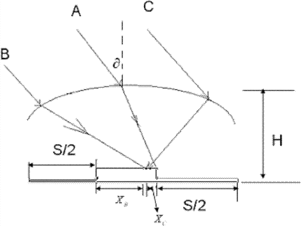
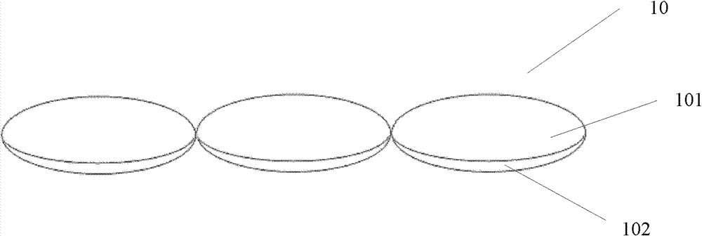
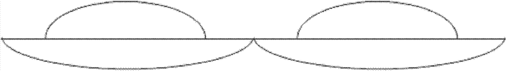
[0059] The present invention proposes a double-sided microlens array to increase the field angle of the microlens array and shorten the focal length of the microlens array. Such as figure 2 As shown, the double-sided microlens array may specifically include: an array of double-sided microlenses 10, wherein each double-sided microlens 10 in the array includes an upper microconvex lens 101 and a lower microconvex lens 102; each double-sided microlens In 10, the upper microconvex lens 101 and the lower microconvex lens 102 are arranged in a one-to-one correspondence with the center, and the corresponding upper microconvex lens 101 and the lower microconvex lens 102 are bonded together.

[0060] In the embodiment of the present invention, by setting each microlens in the microlens array as a double-sided microlens including an upper microconvex lens and a lower microconvex lens, the incident light can be focused twice, which greatly shortens the focal length; After the incident ligh...

Embodiment 2

[0068] In the embodiment of the present invention, the manufacturing method of the above-mentioned double-sided microlens array is shown, such as Figure 7 As shown, the method may include the following processing steps:

[0069] Step 101: Provide a substrate;

[0070] Step 102, etching a cavity array with the same width as the double-sided microlens on the substrate;

[0071] For simple representation, only one microlens in the double-sided microlens array is taken as an example, such as Picture 8 As shown, 801 is a substrate, usually silicon; 802 is a cavity with a uniform shape formed by etching on a silicon substrate;

[0072] Step 103: In each cavity, a concave surface required for making the lower micro-convex lens is formed by anisotropic etching; the concave surface is such as Picture 8 Shown in 803;

[0073] Step 104: Inject a second material for forming the lower layer of micro-convex lenses and a first material for forming the upper layer of micro-convex lenses into the con...


PUM


Abstract

The invention discloses a double-sided microlens array and a manufacturing method thereof. The double-sided microlens array comprises an array formed by double-sided microlens; each double-sided microlens in the array comprises an upper-layer micro convex lens and a lower-layer micro convex lens; the upper-layer micro convex lens and the lower-layer micro convex lens of each double-sided microlens are in the central one-to-one array form; and the upper-layer micro convex lenses and the lower-layer micro convex lenses are adhered together. According to the embodiment of the invention, the angel of field of the microlens array can be increased greatly, and the focal length of the microlens array can be shortened.

Description

Technical field [0001] The invention relates to the technical field of optical device manufacturing, in particular to a double-sided microlens array and a manufacturing method thereof. Background technique [0002] The integration of microlens arrays (MLA, microlens array) and various devices to achieve light-gathering or imaging functions is a popular direction in the research of micro-optical systems in recent years. As for the non-imaging microlens array that mainly acts as a concentrator, how can all incident light enter the photosensitive absorption area? From the perspective of geometric optics, the fundamental basis for the design of the energy-collecting microlens is: given the pixel size, the size of the photosensitive area of ​​the detector, the F number of the front optical system, the refractive index and wavelength of the lens material, etc. Some structural parameters of a single microlens are obtained, so that the energy of incident light falling in the photosensit...

Claims


Application Information

Patent Timeline
Patent Type & Authority Applications(China)
IPC IPC(8): G02B3/00G03F7/20
Inventor 闫建华欧文欧毅
Owner 北京中科微投资管理有限责任公司
Why Eureka
Try Eureka