Silicon wafer surface cleaning device of solar cell printer

A technology on the surface of solar cells and silicon wafers, applied to the general parts of printing machinery, printing machines, printing, etc., can solve the problems of reducing the printing yield and increasing the production cost, so as to improve the printing yield, increase the collection, and improve the photoelectricity The effect of conversion efficiency

Inactive Publication Date: 2012-12-05
EGING PHOTOVOLTAIC TECHNOLOGY CO LTD
View PDF0 Cites 3 Cited by
  • Summary
  • Abstract
  • Description
  • Claims
  • Application Information

AI Technical Summary

Problems solved by technology

[0002] With the development and application of solar energy, silicon solar cells are widely used in the photovoltaic power generation industry. The printing process is an important link in the manufacture of traditional crystalline silicon solar cells. Usually, solar cell printers are used to print silicon wafers on solar cells. Printing is carried out on the feeding belt of the printing machine, and there are often silicon nitride particles on the surface of the silicon wafer. If these particles are not removed during the printing process, the printing screen will be punctured, thereby reducing the printing yield, and the production cost will be reduced accordingly. Increase

Method used


Image

  • Silicon wafer surface cleaning device of solar cell printer
  • Silicon wafer surface cleaning device of solar cell printer
  • Silicon wafer surface cleaning device of solar cell printer

Examples


Embodiment Construction

[0012] The present invention is described in further detail now in conjunction with accompanying drawing. These drawings are all simplified schematic diagrams, which only illustrate the basic structure of the present invention in a schematic manner, so they only show the configurations related to the present invention.

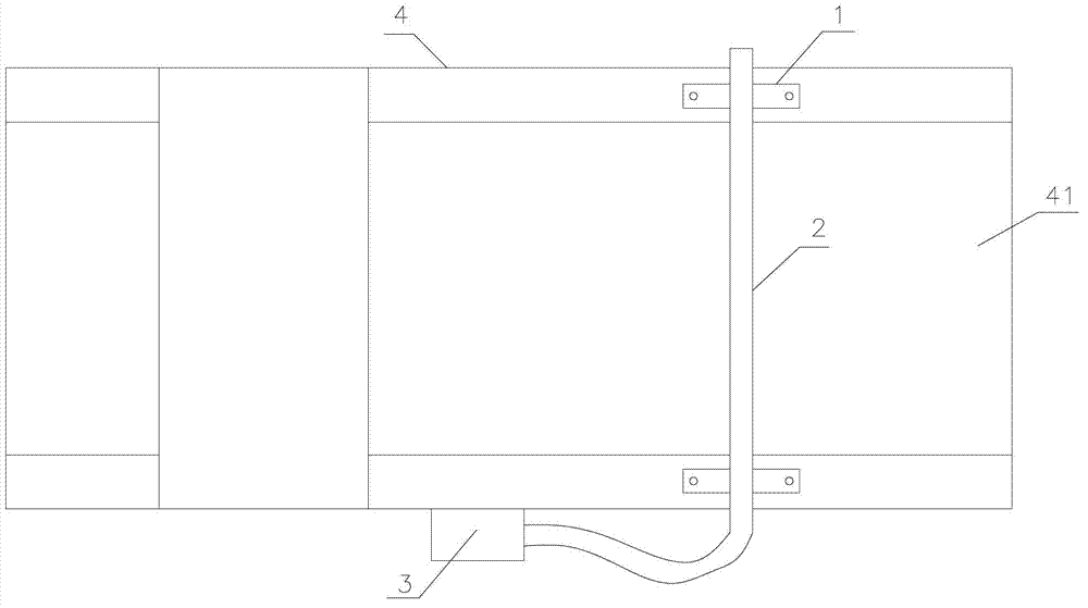
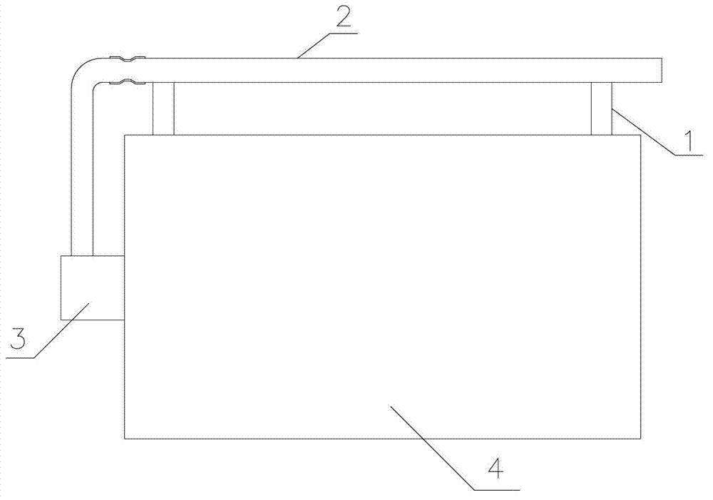
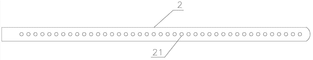
[0013] like Figure 1~3 The structural representation of the specific embodiment of the silicon wafer surface cleaning device of the solar cell printing machine shown in the present invention comprises support 1, air blowing pipe 2 and gas source 3, and the mouth of mouth of air blowing pipe 2 is closed at one end, and the mouth of another end is open, The mouth of the open air blowing pipe 2 is connected to the air source 3 through the pipeline. There are a plurality of air blowing holes 21 on the pipe wall of the air blowing pipe 2. The plurality of air blowing holes 21 are equally spaced on the pipe wall of the air blowing pipe 2. The air source 3 It is ar...


PUM


Abstract

The invention relates to a silicon wafer surface cleaning device of a solar cell printer. The silicon wafer surface cleaning device of the solar cell printer comprises a bracket, a blowing pipe and an air source; a pipe opening at one end of the blowing pipe is sealed; an pipe opening at the other end of the blowing pipe is open; the opened pipe opening of the blowing pipe is communicated with the air source through a pipeline; a plurality of blowing holes are arranged on the pipe wall of the blowing pipe; the air source is arranged on the solar cell printer; the brackets are arranged at the two sides of a conveyer belt of the solar cell printer, and the blowing pipe is arranged on the bracket. The silicon wafer surface cleaning device of the solar cell printer carries out cleaning work right opposite to a silicon wafer by adding the blowing pipe on the conveyer belt of the solar cell printer, blowing air through the air source and ventilating through the blowing holes, and can blow away silicon nitride particles and the like on the silicon wafer surface, so that the printing yield is improved, and collection of current on the silicon surface is increased, thereby improving the photoelectric conversion efficiency.

Description

technical field [0001] The invention relates to the technical field of solar cell printing devices, in particular to a silicon chip surface cleaning device for a solar cell printing machine. Background technique [0002] With the development and application of solar energy, silicon solar cells are widely used in the photovoltaic power generation industry. The printing process is an important link in the manufacture of traditional crystalline silicon solar cells. Usually, solar cell printers are used to print silicon wafers on solar cells. Printing is carried out on the feeding belt of the printing machine, and there are often silicon nitride particles on the surface of the silicon wafer. If these particles are not removed during the printing process, the printing screen will be punctured, thereby reducing the printing yield, and the production cost will be reduced accordingly. Increase. Contents of the invention [0003] The technical problem to be solved by the present i...

Claims


Application Information

Patent Timeline
Patent Type & Authority Applications(China)
IPC IPC(8): B41F23/00
Inventor 胡琴
Owner EGING PHOTOVOLTAIC TECHNOLOGY CO LTD
Why Eureka
Try Eureka