Check patentability & draft patents in minutes with Patsnap Eureka AI!

Metal oxide semiconductor (MOS) type power semiconductor device

A power semiconductor and device technology, applied in the field of MOS type semiconductor power device structure, can solve the problems of destructive failure of power devices, secondary breakdown of parasitic transistors, shortened service life, etc. Capacitance reduction and reliability improvement effect

Inactive Publication Date: 2012-12-19
UNIV OF ELECTRONIC SCI & TECH OF CHINA
View PDF2 Cites 8 Cited by
  • Summary
  • Abstract
  • Description
  • Claims
  • Application Information

AI Technical Summary

Problems solved by technology

[0006] The technical problem to be solved by the present invention is to trigger the parasitic transistor to turn on and cause secondary breakdown in the case of avalanche multiplication or ESD discharge of the MOS type power semiconductor device, resulting in destructive failure of the power device, reduced service life and reduced reliability The problem of providing a highly reliable power semiconductor device structure

Method used


Image

  • Metal oxide semiconductor (MOS) type power semiconductor device
  • Metal oxide semiconductor (MOS) type power semiconductor device
  • Metal oxide semiconductor (MOS) type power semiconductor device

Examples


Embodiment Construction

[0020] In order to make the technical problems, technical solutions and beneficial effects to be solved by the present invention clearer, the present invention will be further described in detail below in conjunction with the accompanying drawings and embodiments. It should be understood that the specific embodiments described here are only used to explain the present invention, not to limit the present invention.

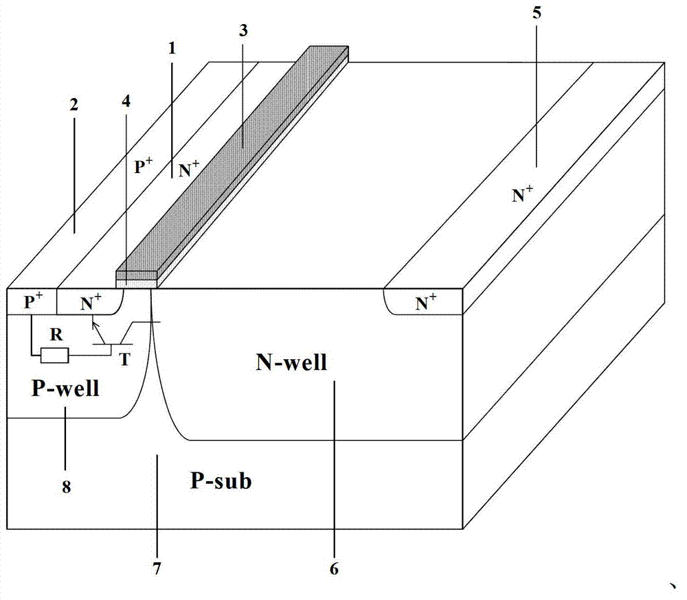
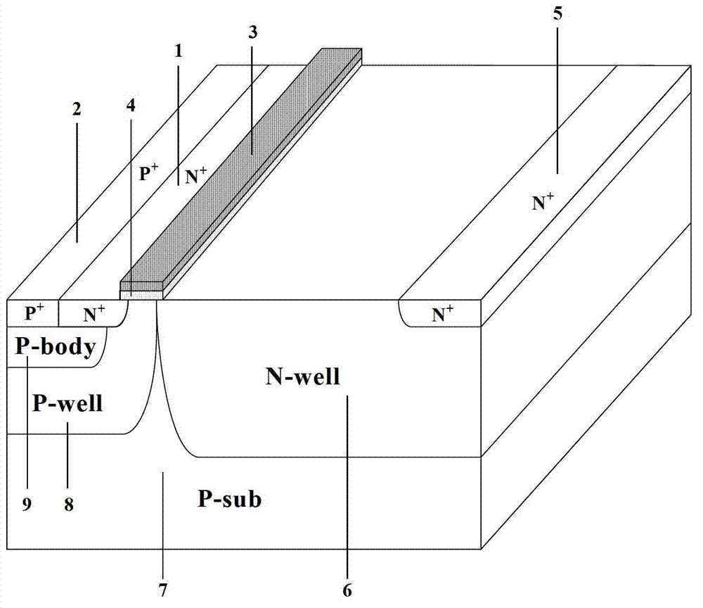
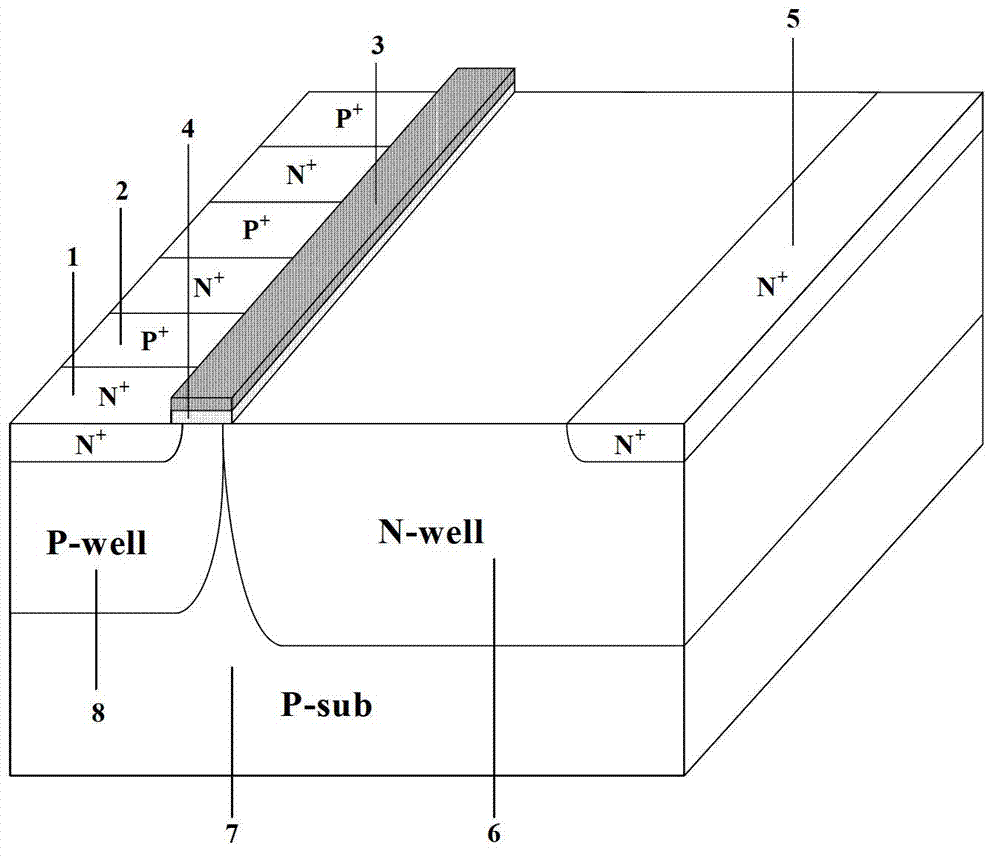
[0021] The MOS type power semiconductor device provided by the present invention changes the structure of the P type impurity heavily doped region 2 and the N type impurity heavily doped region 1 in contact with the cathode metal in the cathode structure of the traditional MOS type power device. Change the P-type impurity heavily doped region 2 and N-type impurity heavily doped region 1 that are located side by side in the P-type well region in a conventional MOS power semiconductor device in a striped structure along the device width direction to be alternately spa...


PUM


Abstract

A metal oxide semiconductor (MOS) type power semiconductor device belongs to the technical field of semiconductor devices. A P-type impurity heavily doped area 2 and an N-type impurity heavily doped area 1 which are of strip structures, which are positioned side by side in a P-type trap area along the width direction of the device and are arranged in the conventional MOS type power semiconductor device are changed to be alternately distributed at intervals along the width direction of the device. With the MOS type power semiconductor device, the starting probability of a parasitic transistor can be greatly reduced, accordingly, the device is effectively prevented from secondary breakdown, the safety working area of the device is widened, and the reliability of the device is improved. Moreover, a parasitic gate source capacitance is reduced by about a half of that of the conventional structure. Finally, injection photomasks of the P-type impurity heavily doped area 2 and the N-type impurity heavily doped area 1 are only needed to be changed during the manufacturing process, so the reliability of the device can be greatly improved, and the MOS type power semiconductor device is simple and practicable.

Description

technical field [0001] The invention belongs to the technical field of semiconductor power devices and relates to the structure of MOS type semiconductor power devices. technical background [0002] In the design of semiconductor power devices, the structural design of the device is very important. Reasonable device structure design can effectively compensate for the impact of material defects and parasitic effects on device performance, avoid local thermoelectricity and secondary breakdown, thereby preventing device failure, extending service life, and improving device reliability. On the contrary, unreasonable device structure design will seriously restrict the reliability of the device. [0003] With the increase of integration and the reduction of process line width, the failure caused by thermoelectric effect on power devices becomes more and more prominent. For metal-oxide-semiconductor (MOS) power devices, secondary breakdown caused by parasitic transistor turn-on i...

Claims


Application Information

Patent Timeline
IPC IPC(8): H01L29/78H01L29/06H01L29/739
CPCH01L29/7835H01L29/0847H01L29/0619
Inventor 乔明何逸涛温恒娟向凡周锌吴文杰张波
Owner UNIV OF ELECTRONIC SCI & TECH OF CHINA
Features
  • R&D
  • Intellectual Property
  • Life Sciences
  • Materials
  • Tech Scout
  • Unparalleled Data Quality
  • Higher Quality Content
  • 60% Fewer Hallucinations
Learn More