Mobile communication terminal, embedded PCB (printed circuit board) structure and processing method of embedded PCB structure

A PCB board and embedded technology, which is applied in the field of mobile communication terminals, embedded PCB board structure and its processing, can solve the problems affecting the thickness of smart products, and achieve the effect of reducing the thickness of the whole machine

Inactive Publication Date: 2012-12-19
HUIZHOU TCL MOBILE COMM CO LTD
View PDF6 Cites 11 Cited by
  • Summary
  • Abstract
  • Description
  • Claims
  • Application Information

AI Technical Summary

Problems solved by technology

[0004] In view of the above-mentioned deficiencies in the prior art, the object of the present invention is to provide a mobile communication terminal, an embedded PCB...

Method used


Image

  • Mobile communication terminal, embedded PCB (printed circuit board) structure and processing method of embedded PCB structure
  • Mobile communication terminal, embedded PCB (printed circuit board) structure and processing method of embedded PCB structure
  • Mobile communication terminal, embedded PCB (printed circuit board) structure and processing method of embedded PCB structure

Examples


Embodiment Construction

[0026] The present invention provides a mobile communication terminal, an embedded PCB board structure and a processing method thereof. In order to make the purpose, technical solution and effect of the present invention clearer and clearer, the present invention will be further described in detail below. It should be understood that the specific embodiments described here are only used to explain the present invention, not to limit the present invention.

[0027] The invention provides a method for processing the embedded PCB structure, the steps of which are:

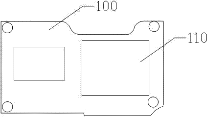
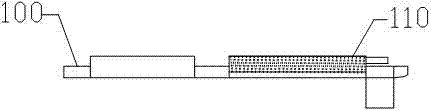
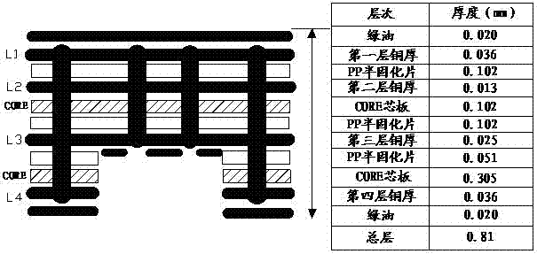
[0028] A groove for embedding devices is provided on the PCB, and pads for welding the devices are embedded in the inner layer of the groove, and the PCB is configured to have a multi-layer PCB sublayer structure. The embedded PCB board structure made by the above method, such as figure 1 and figure 2 As shown, it includes: a PCB board 100 on which a groove 110 for embedding devices is arranged.

[0029] The impro...


PUM

PropertyMeasurementUnit
Depthaaaaaaaaaa
Depthaaaaaaaaaa

Abstract

The invention discloses a mobile communication terminal, an embedded PCB (printed circuit board) structure and a processing method of the embedded PCB structure. The processing method of the embedded PCB structure includes steps of setting a groove used for embedding a device on a PCB with a plurality of PCB sublayers, and embedding a welding plate used for welding the device on the inner layer of the groove. By taking the PCB of smart products as research objects, a large chip limited by height is embedded in the PCB, and the integral thickness of the mobile communication terminal is reduced.

Description

technical field [0001] The invention relates to the field of PCB structure, in particular to a mobile communication terminal, an embedded PCB structure and a processing method thereof. Background technique [0002] With the widespread application of smart products such as mobile phones, the competition among smart product manufacturers is becoming more and more fierce. Each manufacturer will launch several products with different characteristics every year, and the thickness of the product has become a selling point for various manufacturers to promote. Taking mobile phones as an example, the thickness of mobile phones has gradually become thinner, and has reached a thickness of 10mm or less. However, due to the limitations of the motherboard and device thickness, it is very difficult to further reduce the thickness. On the other hand, the thickness is small. Advanced devices are expensive, and some ultra-thin technologies are only mastered by a few manufacturers, all of whi...

Claims


Application Information

Patent Timeline
IPC IPC(8): H05K1/18H05K3/34H04M1/02
Inventor 王佳
Owner HUIZHOU TCL MOBILE COMM CO LTD
Why Eureka
Try Eureka