LED (Light Emitting Diode) flip chip structure and manufacturing method thereof

A manufacturing method and technology of LED chips, applied to electrical components, electric solid devices, circuits, etc., can solve problems such as overflow flowing into LED chips, short circuit, etc.

Inactive Publication Date: 2012-12-26
SCIENBIZIP CONSULTINGSHENZHENCO
View PDF3 Cites 14 Cited by
  • Summary
  • Abstract
  • Description
  • Claims
  • Application Information

AI Technical Summary

Problems solved by technology

In this LED flip-chip structure, solder is usually used between the electrodes of the LED chip and the electrodes of the substrate. However, the solder is likely to overflow and flow between the electrodes of the LED chip due to high temperature melting during the soldering process. resulting in short circuit etc.

Method used


Image

  • LED (Light Emitting Diode) flip chip structure and manufacturing method thereof
  • LED (Light Emitting Diode) flip chip structure and manufacturing method thereof

Examples


Embodiment Construction

[0015] The present invention will be further described in detail below in conjunction with the accompanying drawings.

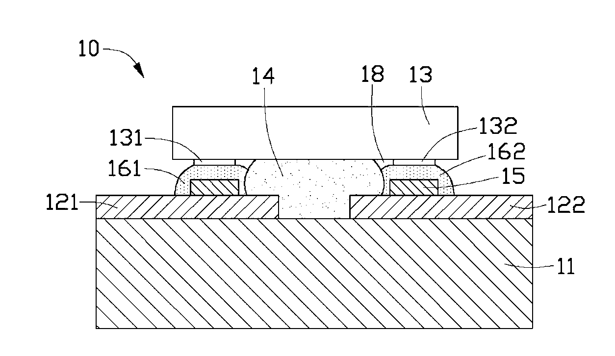
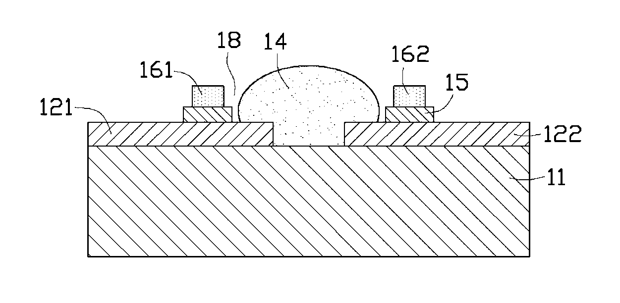
[0016] see figure 1 , an LED flip-chip structure 10 provided in an embodiment of the present invention includes a substrate 11 , a circuit layer 12 , an LED chip 13 and a blocking structure 14 .

[0017] The substrate 11 is used to support the LED chips 13 thereon. The substrate 11 is flat, and its material is a silicon wafer.

[0018] The circuit layer 12 is formed on the upper surface of the substrate 11, the circuit layer 12 includes a first electrode 121 and a second electrode 122 insulated from each other and is formed on the upper surface of the first electrode 121 and the second electrode 122 respectively. The metal gasket 15. The metal pads 15 are arranged corresponding to the electrodes of the LED chip 13 , and play a role of positioning and supporting the LED chip 13 . During specific implementation, the metal pad 15 may not be formed on the fir...


PUM


Abstract

The invention discloses an LED (Light Emitting Diode) flip chip structure comprising a substrate, a circuit layer formed on the substrate, and an LED chip located on the circuit layer, wherein the circuit layer comprises a first electrode and a second electrode which are insulated with each other; the LED chip comprises a positive electrode and a negative electrode which are correspondingly connected with the first electrode and the second electrode of the circuit layer respectively; the positive electrode and the negative electrode are connected with the first electrode and the second electrode respectively through solder flip chips; the LED flip chip structure further comprises a barrier structure located between the positive electrode and the negative electrode; and the barrier structure is made of a colloidal insulating material. The invention further relates to a manufacturing method of the LED (Light Emitting Diode) flip chip structure.

Description

technical field [0001] The invention relates to a semiconductor structure, in particular to an LED flip-chip structure and a manufacturing method thereof. Background technique [0002] Many of the current LED packaging structures use flip-chip structures to fix LED chips. In this LED flip-chip structure, solder is usually used between the electrodes of the LED chip and the electrodes of the substrate. However, the solder is likely to overflow and flow between the electrodes of the LED chip due to high temperature melting during the soldering process. This may cause a short circuit or the like. Contents of the invention [0003] In view of this, it is necessary to provide an LED flip-chip structure and a manufacturing method thereof that prevent solder overflow. [0004] An LED flip-chip structure includes a substrate, a circuit layer formed on the substrate and an LED chip located on the circuit layer. The circuit layer includes a first electrode and a second electrode ...

Claims


Application Information

Patent Timeline
Patent Type & Authority Applications(China)
IPC IPC(8): H01L33/48H01L33/56H01L33/00
CPCH01L2924/0002H01L33/486H01L33/62H01L2933/0066H01L2224/16
Inventor 沈佳辉洪梓健
Owner SCIENBIZIP CONSULTINGSHENZHENCO
Why Eureka
Try Eureka