Display module
A display and display panel technology, applied to static indicators, instruments, electric solid devices, etc., can solve problems such as short circuit, lower yield rate, and higher manufacturing cost
- Summary
- Abstract
- Description
- Claims
- Application Information
AI Technical Summary
Problems solved by technology
Method used
Image
Examples
Embodiment 1
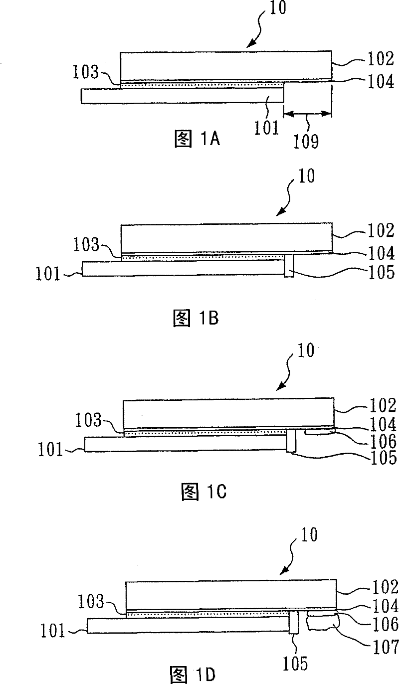
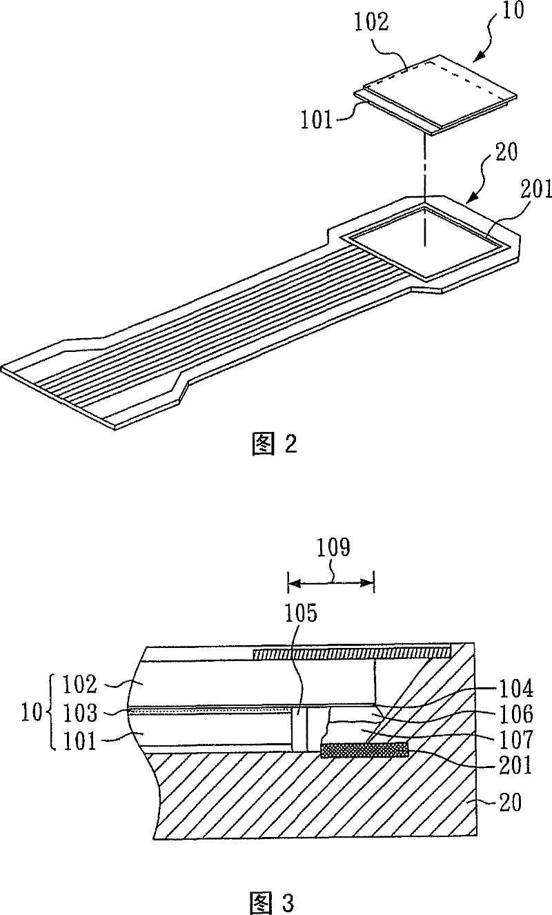
[0029] Such as image 3 Shown is a cross-sectional view of the structure of the display module of this embodiment, which includes: a display panel 10 , a transparent electrode layer 104 , a casing 20 , a conductive glue 107 , a solder layer 106 , and an insulating glue 105 . The display panel 10 includes a lower substrate 101 , an upper substrate 102 , and a liquid crystal layer 103 . Wherein, the upper substrate 101 and the lower substrate are disposed opposite to each other, and the liquid crystal layer 103 is disposed between the upper substrate 101 and the lower substrate 102 . Moreover, the display panel 10 has a dislocation portion 109 , and the transparent electrode layer 104 is disposed on the upper substrate 102 and extends to the dislocation portion 109 . On the other hand, the housing 20 has a conductive line 201 . In addition, the conductive glue 107 is connected to the transparent electrode layer 104 and the conductive circuit 201 . The solder layer 106 is form...
Embodiment 2
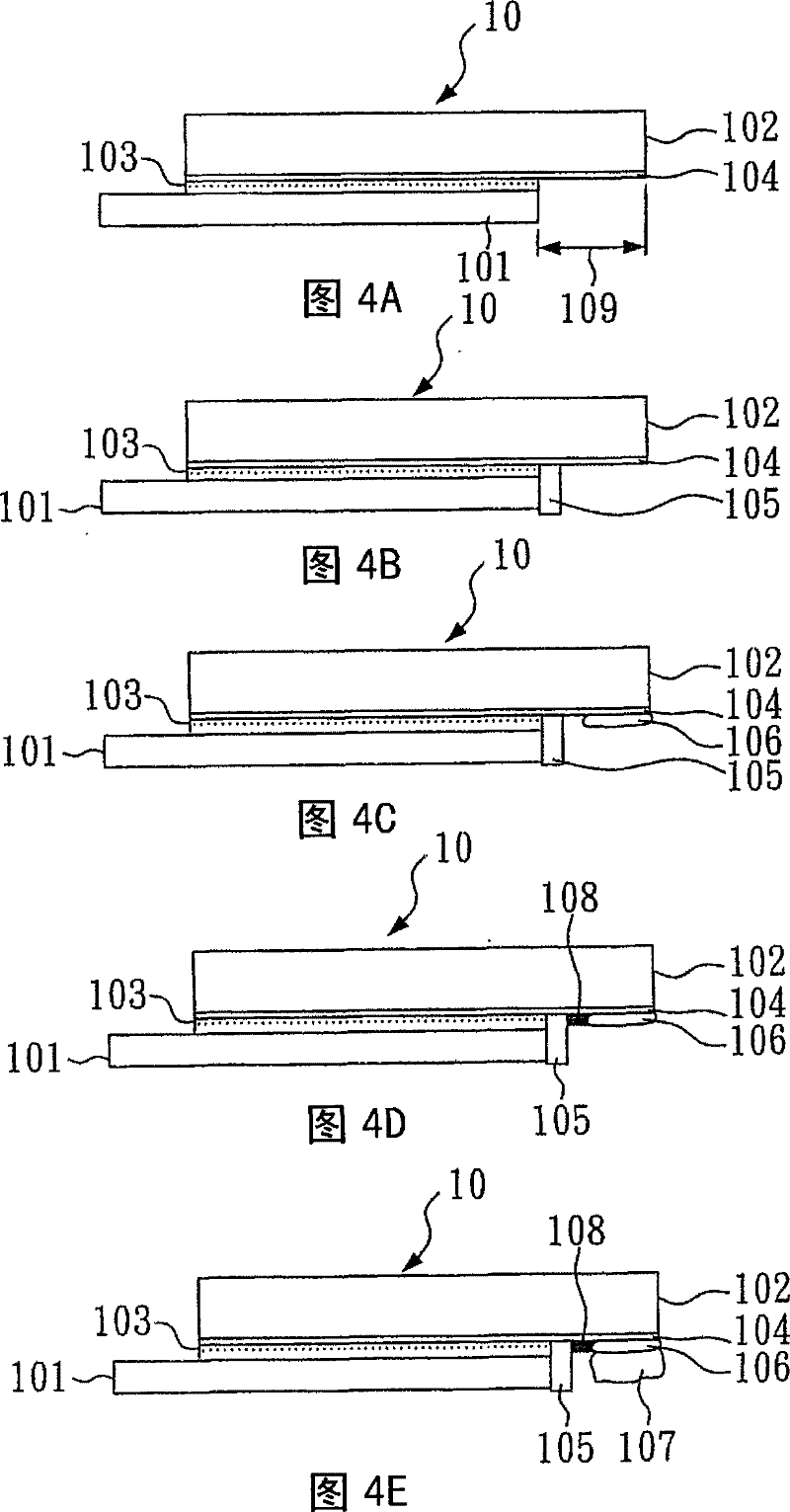
[0036] Please refer to Figure 4 to Figure 5 , is the flow chart of manufacturing the display module of this embodiment. The manufacturing method of this embodiment is roughly the same as that of Embodiment 1, but the difference lies in that the reference Figure 4D Shown: after the step of coating the solder layer 106 , coat the solder resist layer 108 between the insulating glue 105 and the solder layer 106 . Next, the solder resist layer 108 (not shown) is hardened. In this embodiment, the method of hardening the solder resist layer 108 is thermal hardening. The solder resist layer 108 in this embodiment has the effect of strengthening the blocking of overflowing solder paste, and can further enhance the effect of preventing the electrical conduction between the upper substrate 102 and the lower substrate 101 .
[0037] The structure of the display module of this embodiment is substantially the same as that of Embodiment 1, but the structure of the display module of this...
PUM
 Abstract
Description
Claims
Application Information


