Method for producing resinous multilayer substrate
A technology of multilayer substrate and manufacturing method, which is applied in the direction of multilayer circuit manufacturing, printed circuit manufacturing, printed circuit, etc., can solve the problems of no via hole filling manufacturing method, no masking carrier film, etc., and achieve the suppression of short circuit defects , Suppress the effect of splashing and suppressing undulations
- Summary
- Abstract
- Description
- Claims
- Application Information
AI Technical Summary
Problems solved by technology
Method used
Image
Examples
Embodiment approach 1
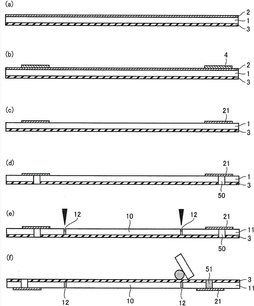
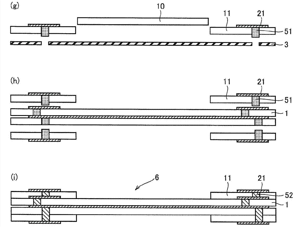
[0038] refer to figure 1 with figure 2 An example of the present invention will be described.
[0039] (pasting process)
[0040] First, if figure 1 As shown in (a), the conductor layer 2 is formed on one surface of the insulating substrate (insulating sheet) 1, and the carrier film 3 is attached so that peeling is possible on the other surface. Preferably, the carrier film has some holding power and is slightly adhesive when stretched without undue force.
[0041] The insulating substrate 1 contains thermoplastic resin. Examples of thermoplastic resins include polyimide, liquid crystal polymer (LCP), polyetherketone resin (PEEK), and polyphenylene sulfide resin (PPS). When the insulating substrate contains a thermoplastic resin, since the resin tends to flow by heat treatment, it is preferable that the heat treatment such as stamping (batch thermocompression bonding) after lamination be relatively low temperature.
[0042] As the material of the conductor layer 2, for ...
Embodiment approach 2
[0074] In this embodiment, the shape (cavity portion) of a part (unnecessary portion 10) of the insulating substrate cut out by the slit includes at least one corner portion ( Image 6 (b)). Image 6 (b), from Image 6 The shape shown in (a) has an R with the corners removed. This embodiment differs from Embodiment 1 in this point, and is the same as Embodiment 1 in other respects. In addition, the shape here means the shape seen from the normal direction of the principal surface of an insulating substrate.
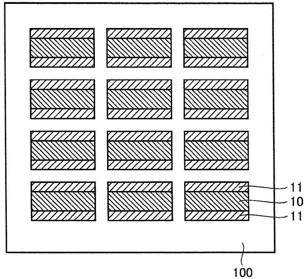
[0075] In addition, the insulating substrate 11 including the unnecessary portion 10 of such a shape is, for example, Figure 7 As shown, a plurality of substrate base materials 100 can be used for simultaneous production.
[0076] At least one part of the corner (corner part) of the cutting part (unnecessary part 10) is provided with R (the shape of the circumferential part having a predetermined curvature radius R), so that insulation can be prevented during transpo...
PUM
 Abstract
Description
Claims
Application Information


