Thickness tester structure for measuring thickness of wafer during grinding

A wafer thickness and thickness gauge technology, applied in mechanical thickness measurement and other directions, can solve the problems of large measurement error value, process loss, product yield decline, etc., to reduce measurement errors, avoid debris, and improve product yield Effect

Active Publication Date: 2013-01-02
WUXI RED MICROELECTRONICS CORP
View PDF5 Cites 6 Cited by
  • Summary
  • Abstract
  • Description
  • Claims
  • Application Information

AI Technical Summary

Problems solved by technology

[0002] Existing thickness gauges such as figure 1 , when measuring the thickness of the wafer, the central axis of the wafer 1 must be perpendicular to the measurement support 2, and the micrometer screw 4 of the micrometer 3 is placed horizontally, and the measurement of the reference seat 5 and the micrometer screw 4 of the measurement support 2 The ends are aligned with each other, and the measurement support 2 is supported on the base 6. The measurement needs to take multi-point measurement. When measuring the thickness of the corner of the wafer, sometimes the measurement end of the micrometer screw 4 of the micrometer 3 cannot clamp the wafer 1. The falling of wafer 1 causes wafer 1 to break, causing serious process loss; when the micrometer 3 clamps the blue-coated silicon wafer, because the micrometer 3 is pressed by hand to measure, the blue film will sink and the measurement value will be wrong. In addition, the vertical measurement of wafer 1 will also cause a large measurement error value due to the shaking of wafer 1, which will have a great impact on the control of wafer loading and bonding in the next process, resulting in a decline in product yield

Method used


Image

  • Thickness tester structure for measuring thickness of wafer during grinding
  • Thickness tester structure for measuring thickness of wafer during grinding
  • Thickness tester structure for measuring thickness of wafer during grinding

Examples


Embodiment Construction

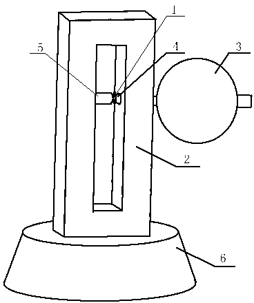
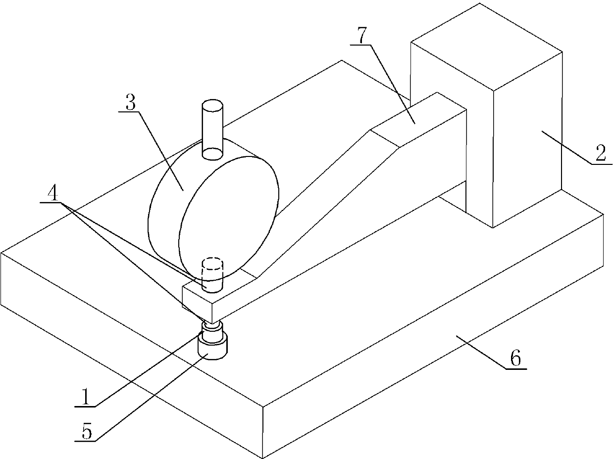
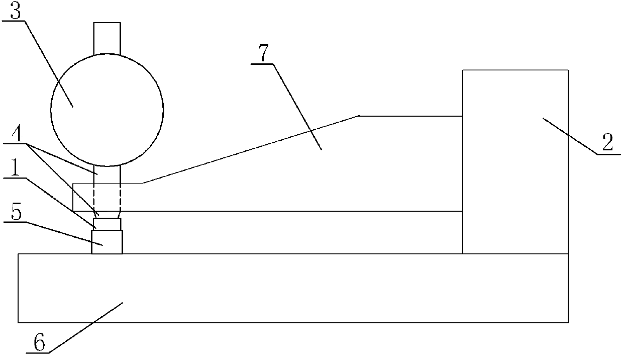
[0009] see figure 2 , image 3 , Including the base 6, the micrometer 3, the wafer 1, the base 6 is arranged horizontally, the vertical plate 2 is supported on the upper end surface of the base 6, one end of the horizontal supporting plate 7 is fastened to one side of the vertical plate 2, and one end of the horizontal supporting plate 7 The measuring end of the micrometer screw 4 provided with the micrometer 3 and the micrometer 3 penetrates the transverse support plate 7 and then vertically faces the upper end surface of the base 6. The micrometer screw 4 is provided with a reference seat 5 corresponding to the upper end surface of the base 6. The micrometer screw 4, The wafer 1 is arranged in the gap between the reference base 5, the upper end surface of the wafer 1 is close to the measuring end of the micrometer screw 4, and the lower end surface of the wafer 1 is close to the upper end surface of the reference base 5.


PUM


Abstract

The invention provides a thickness tester structure for measuring the thickness of a wafer during grinding. By the thickness tester structure, a fragment situation caused by the falling of the wafer is avoided, and the process loss is reduced; and during measuring, the measurement errors of the wafer are reduced, and the product yield is improved. The thickness tester structure comprises a base, a micrometer and a wafer, and is characterized in that the base is horizontally arranged; an upright plate is supported on the upper end face of the base; one end of a transverse supporting plate is tightly connected with one side of the upright plate; the micrometer is arranged at one end of the transverse supporting plate; a measuring end of a micrometric screw of the micrometer penetrates through the transverse supporting plate, and then vertically faces the upper end face of the base; a benchmark seat is arranged on the micrometric screw corresponding to the upper end face of the base; the wafer is arranged in a gap between the micrometric screw and the benchmark seat; the upper end face of the wafer is clung to the measuring end of the micrometric screw; and the lower end face of the wafer is clung to the upper end face of the benchmark seat.

Description

Technical field [0001] The invention relates to the technical field of wafer measurement for semiconductor device packaging, in particular to a thickness gauge structure used for measuring the thickness of a wafer during a grinding process. Background technique [0002] Existing thickness gauges such as figure 1 When measuring the thickness of the wafer, the center axis of the wafer 1 must be perpendicular to the measuring support 2, and the micrometer screw 4 of the micrometer 3 is placed horizontally, and the measurement of the reference base 5 and the micrometer screw 4 of the measuring support 2 The measuring support 2 is supported on the base 6. Multi-point measurement is required for measurement. When measuring the thickness of the corners of the wafer, sometimes the measuring end of the micrometer screw 4 of the micrometer 3 cannot clamp the wafer 1 The falling of wafer 1 causes wafer 1 to break, causing serious process loss; when the micrometer 3 clamps the silicon wafer ...

Claims


Application Information

Patent Timeline
Patent Type & Authority Applications(China)
IPC IPC(8): G01B5/06
Inventor 陆振
Owner WUXI RED MICROELECTRONICS CORP
Why Eureka
Try Eureka