Testing device of 3D-SIC (Three-Dimensional-Semiconductor Integrated Circuit) through silicon vias provided with signal rebounding module

A through-silicon via and signal bounce technology, which is applied in the field of 3D-SIC through-silicon via test equipment, can solve problems such as the difficulty of effective detection of failed TSVs, and achieve low power consumption, small area, and low practical cost.

Active Publication Date: 2013-01-02
HEFEI UNIV OF TECH
View PDF4 Cites 13 Cited by
  • Summary
  • Abstract
  • Description
  • Claims
  • Application Information

AI Technical Summary

Problems solved by technology

[0015] The present invention provides a 3D-SIC through-silicon via test device provided with a signal bounce module to avoid the shortcomings of the above-mentioned prior art, so as to solve the problem of effectively testing the failed TSV in the 3D chip manufacturing process. Detecting Difficult Issues

Method used


Image

  • Testing device of 3D-SIC (Three-Dimensional-Semiconductor Integrated Circuit) through silicon vias provided with signal rebounding module
  • Testing device of 3D-SIC (Three-Dimensional-Semiconductor Integrated Circuit) through silicon vias provided with signal rebounding module
  • Testing device of 3D-SIC (Three-Dimensional-Semiconductor Integrated Circuit) through silicon vias provided with signal rebounding module

Examples


Embodiment Construction

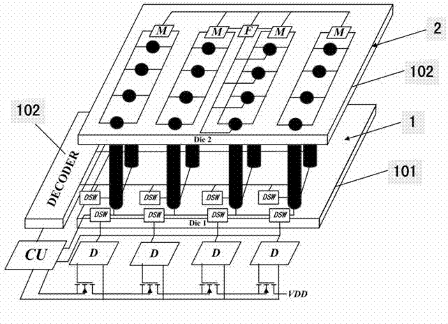
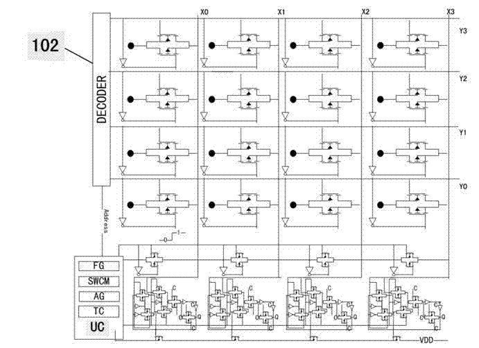
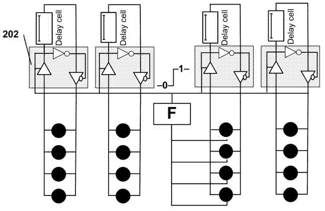
[0031] join Figure 1 ~ Figure 4 , a 3D-SIC through-silicon via testing device provided with a signal bounce module, including a transmitting end 1 and a receiving end 2; the transmitting end and the receiving end are connected through a plurality of through-silicon vias TSV; the transmitting end includes a first chip under test 101, a decoder 102, a control unit CU, a latch D and a bidirectional switch DSW; the receiving end 2 includes a second chip under test 201 and a signal bounce module; the signal bounce module includes a A signal generator F, a plurality of delay units M and a plurality of tri-state gates 202;

[0032] The upper end of the TSV is connected to the delay unit M and the signal generator F at the receiving end, and the delay units M are connected to the signal generator F through respective tri-state gates 202;

[0033]The lower end of the TSV is connected to the decoder 102 and the bidirectional switch DSW at the sending end; the decoder 102, the latch D ...


PUM


Abstract

The invention discloses a testing device of a 3D-SIC (Three-Dimensional-Semiconductor Integrated Circuit) through silicon vias provided with a signal rebounding module. A sending end is connected with a receiving end by through a plurality of silicon vias TSVs. The sending end comprises a first tested chip, a decoder, a control unit CU, a latch D and a bidirectional switch DSW. The receiving end comprises a second tested chip and a signal rebounding module. The signal rebounding module comprises a signal generator F, a plurality of delay cells and a plurality of three-state gates. The upper ends of the TSVs are connected with the delay cells M and the signal generator F at the receiving end. The lower ends of the TSVs are connected with the decoder and the DSW at the sending end. The decoder, the latch D and the DSW are connected with the CU. The latch D is further connected with the DSW. The testing device of the 3D-SIC through silicon vias provided with the signal rebounding module can effectively solve the problem that failed TSVs in the 3D chip preparing process are hard to detect effectively, and has the advantages of smaller area and practical expenses and lower power consumption and the like.

Description

technical field [0001] The invention relates to a testing device for a 3D-SIC passing through silicon vias provided with a signal bounce module. Background technique [0002] With the continuous development of the chip manufacturing process, the size of the chip has been continuously reduced and the performance has been continuously improved, which has continued the glory of Moore's Law for nearly half a century. However, the size of semiconductor transistors is close to the nanometer level, indicating that the chip manufacturing industry will encounter a huge bottleneck, and Moore's Law may fail. In order to continue Moore's Law and continue to improve the performance of chips, 3D chips came into being. In previous integrated circuits, all components are distributed on one plane, which is called 2D integrated circuits. The design of 3D integrated circuits is different from the planar design method of 2D integrated circuits. It stacks multiple chips (Die) vertically and in...

Claims


Application Information

Patent Timeline
Patent Type & Authority Applications(China)
IPC IPC(8): H01L21/66
Inventor 王伟方芳陈田刘军唐勇李润丰
Owner HEFEI UNIV OF TECH
Why Eureka
Try Eureka