Organic light-emitting diode display panel and manufacturing method thereof

A technology for light-emitting diodes and display panels, which is applied in the directions of organic semiconductor devices, semiconductor/solid-state device manufacturing, electrical components, etc., can solve the problem of easy displacement, the inability to fasten the thin film transistor array substrate 101 and the cover plate 102, and the thin film transistor array substrate. 101 and cover plate 102 have low structural strength and other problems, to achieve the effect of enhancing service life, preventing warpage, strong coagulation force and strength

Inactive Publication Date: 2013-01-02
SHENZHEN CHINA STAR OPTOELECTRONICS TECH CO LTD
View PDF6 Cites 7 Cited by
  • Summary
  • Abstract
  • Description
  • Claims
  • Application Information

AI Technical Summary

Problems solved by technology

[0004] Further, after cutting the combination of the thin film transistor array substrate 101 and the cover plate 102, due to the warping of the thin film transistor array substrate 101 or the cover plate 102, the thin film transistor array substrate 101 and the cover plate 102 cannot be fastened, so any one of them Or easily displaced, so that the combination of the thin film transistor array substrate 101 and the cover plate 102 has a low structura...

Method used


Image

  • Organic light-emitting diode display panel and manufacturing method thereof
  • Organic light-emitting diode display panel and manufacturing method thereof
  • Organic light-emitting diode display panel and manufacturing method thereof

Examples


Embodiment Construction

[0028] The description of the following embodiments refers to the attached drawings to illustrate specific embodiments that the present invention can be implemented.

[0029] reference Figure 3A , 3B , 3C, 3D and Figure 4 , Figure 3A , 3B , 3C and 3D are schematic diagrams of the manufacturing method of the organic light emitting diode display panel of the present invention, Figure 4 It is a flowchart of the manufacturing method of the organic light emitting diode display panel of the present invention.

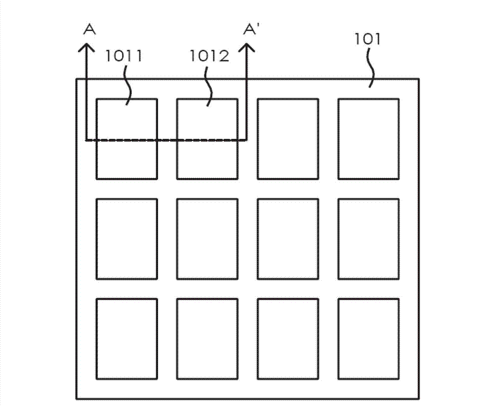
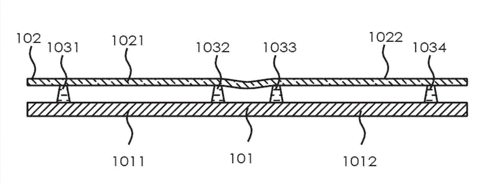
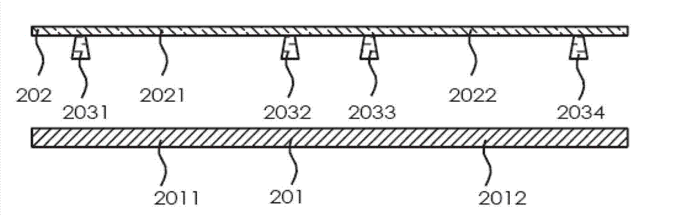
[0030] In step 401, a thin film transistor array substrate 201 and a cover 202 are provided. The thin film transistor array substrate 201 includes a plurality of sub thin film transistor array substrates, such as a first thin film transistor array substrate 2011 and a second thin film transistor array substrate 2012. There is a first connection area between the transistor array substrate 2011 and the second thin film transistor array substrate 2012, and the cover plate 202 is p...


PUM


Abstract

The invention discloses an organic light-emitting diode display panel, which comprises a first thin film transistor array substrate; a first cover plate is arranged on the first thin film transistor array substrate, wherein the first cover plate is provided with first sintering glue and second sintering glue, and an area between the first and the second glue corresponds to the first thin film transistor array substrate; and structural strengthening glue arranged outside the first and the second glue of the first cover plate and contacted with the first thin film transistor array substrate and the first cover plate. The invention further discloses a manufacturing method of the organic light-emitting diode display panel. The invention prevents the phenomenon that the thin film transistor array substrate or the cover plate warps caused by a negative pressure between the thin film transistor array substrate and the cover plate, so that the organic light-emitting diode display panel is more firm and stable in structure.

Description

【Technical Field】 [0001] The present invention relates to the field of organic light emitting diode display technology, in particular to an organic light emitting diode display panel and a manufacturing method thereof. 【Background technique】 [0002] In the manufacturing process of the traditional organic light-emitting diode display panel, a sintering (Frit) glue (1031, 1032, 1033 and 1034) needs to be arranged between the thin film transistor array substrate 101 and the cover plate 102, and the sintering glue is arranged on the thin film transistor array. The edge of the sub-substrates of the substrate 101 (the first thin film transistor array substrate 1011 and the second thin film transistor array substrate 1012), and then the thin film transistor array substrate 101 and the cover plate 102 (the first cover plate 1021 and the second cover plate 1022) The pairing is performed, and then the combination of the thin film transistor array substrate 101 and the cover plate 102 is c...

Claims


Application Information

Patent Timeline
IPC IPC(8): H01L21/77H01L27/32
CPCH01L51/5246H01L21/77H10K71/851H10K71/00H10K59/8722
Inventor 吴泰必
Owner SHENZHEN CHINA STAR OPTOELECTRONICS TECH CO LTD
Why Eureka
Try Eureka