Light emitting device and manufacturing method thereof

A technology of a light-emitting device and a manufacturing method, which is applied to electrical components, electric solid-state devices, circuits, etc., can solve the problems of reducing product yield, overflowing glue, and disadvantages, and achieve the effect of improving product quality and reducing glue overflowing.

Inactive Publication Date: 2013-01-09
GIO OPTOELECTRONICS CORP
View PDF2 Cites 1 Cited by
  • Summary
  • Abstract
  • Description
  • Claims
  • Application Information

AI Technical Summary

Problems solved by technology

Therefore, during the dispensing process, it is more and more easy to cause glue overflow due to the small distance between adjacent LED dies
If it is serious, the glue overflow phenomenon will affect the light shape of the light emitted by the LED die and even affect the electrical connection between the LED die and the substrate, thereby reducing the yield of the product
[0004] However, if the LED die is placed in a reflective housing as a barrier, although it can prevent the glue from overflowing, it will also reduce the light output of the LED die due to the height of the reflective housing itself. angle, which is unfavorable for applications that require a large light output angle

Method used


Image

  • Light emitting device and manufacturing method thereof
  • Light emitting device and manufacturing method thereof
  • Light emitting device and manufacturing method thereof

Examples


Embodiment Construction

[0055] A light emitting device according to a preferred embodiment of the present invention will be described below with reference to related drawings, wherein the same elements will be described with the same reference numerals.

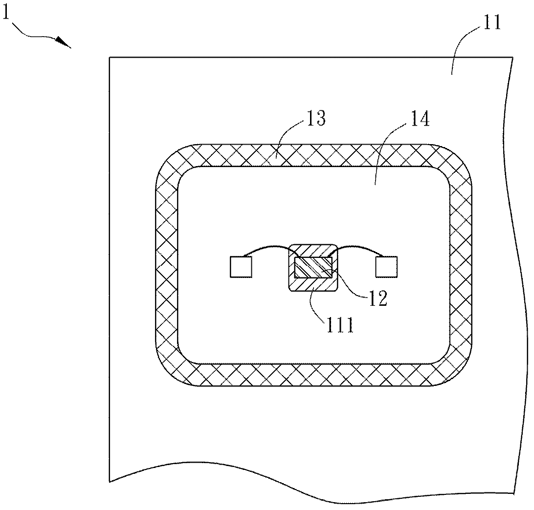
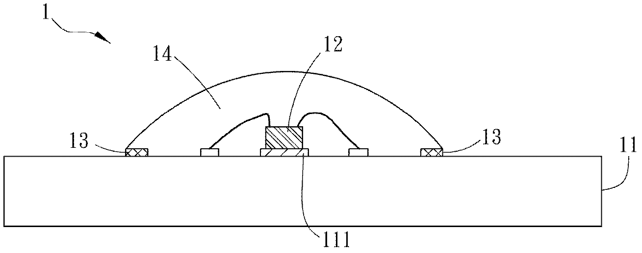
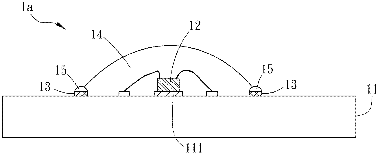
[0056] Please refer to figure 1 and figure 2 as shown, figure 1 is a schematic top view of a light emitting device 1 in a preferred embodiment of the present invention, and figure 2 yes figure 1 side view diagram. The light emitting device 1 includes a substrate 11 , at least one LED die 12 , an encapsulant positioning layer 13 and a first encapsulant 14 . In this embodiment, the light emitting device 1 is an illuminating device as an example, of course, the light emitting device 1 may also be a backlight for a liquid crystal display, a light source for an electronic device, an instruction billboard or an advertisement billboard.

[0057] The substrate 11 has a die setting area 111, wherein the material of the substrate 11 may include, for ex...


PUM


Abstract

A light emitting device comprises a substrate, at least one light emitting diode core, a sealing adhesive positioning layer and a first packaging adhesive body. The substrate is provided with a core setting area, the light emitting diode cores are arranged in the core setting area, the sealing adhesive positioning layer is arranged on the substrate, and at least part of the first packaging adhesive body covers the light emitting diode cores and contacts with the adhesive positioning layer. By the aid of the light emitting device, light emitted from the light emitting diode cores can be prevented from being blocked, and lighting effect can be enhanced.

Description

technical field [0001] The present invention relates to a lighting device, in particular to a lighting device with a light emitting diode. Background technique [0002] In order to increase the production capacity of light-emitting diodes and save production costs, the current packaging process of light-emitting diodes mostly adopts a batch method. Multiple light-emitting diode dies are bonded on a substrate (such as a circuit board, etc.) through die bonding, wire bonding, and dispensing. and other procedures to simultaneously complete the packaging of multiple light-emitting diode dies in one batch process. [0003] At the same time, due to the advancement of semiconductor technology and the continuous pursuit of light, thin, short, and small electronic devices, the size of the substrate is getting smaller and smaller, but the number of LED dies to be arranged on the same substrate is increasing. Therefore, during the dispensing process, it is more and more easy to cause ...

Claims


Application Information

Patent Timeline
Patent Type & Authority Applications(China)
IPC IPC(8): H01L33/52H01L33/48H01L33/00
CPCH01L2224/48091H01L2224/48227H01L2924/181H01L2924/00014H01L2924/00012
Inventor 温俊斌
Owner GIO OPTOELECTRONICS CORP
Why Eureka
Try Eureka