Method for positioning Mark points of PCB (printed circuit board) by image matching

A PCB board and matching method technology, applied in the field of PCB welding visual inspection, can solve the problems of inability to locate the PCB board, inability to quasi-pad welding, inability to accurately calculate the offset of the PCB board, etc., and achieve the effect of high compensation accuracy

Active Publication Date: 2013-01-16
廖怀宝
View PDF5 Cites 21 Cited by
  • Summary
  • Abstract
  • Description
  • Claims
  • Application Information

AI Technical Summary

Problems solved by technology

The shortcomings of these two methods include: when the PCB board is offset, 1. The PCB board cannot be accurately positioned with the existing two detection methods; 2. The PCB board cannot be accurately calculated. Offset; 3. The compensation cannot accurately compensate the PCB board; 4. When soldering the PCB board, it cannot be aligned with the pad for welding

Method used


Image

  • Method for positioning Mark points of PCB (printed circuit board) by image matching
  • Method for positioning Mark points of PCB (printed circuit board) by image matching

Examples


Embodiment Construction

[0017] The technical solution of the present invention will be described in detail below in conjunction with the accompanying drawings.

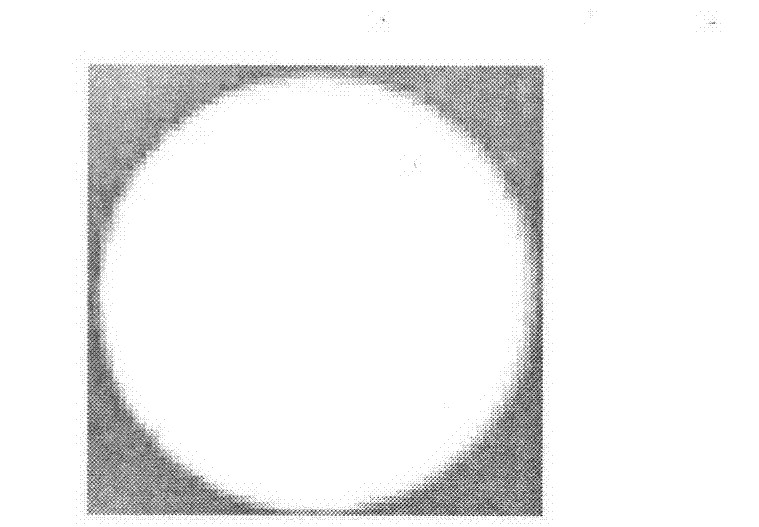
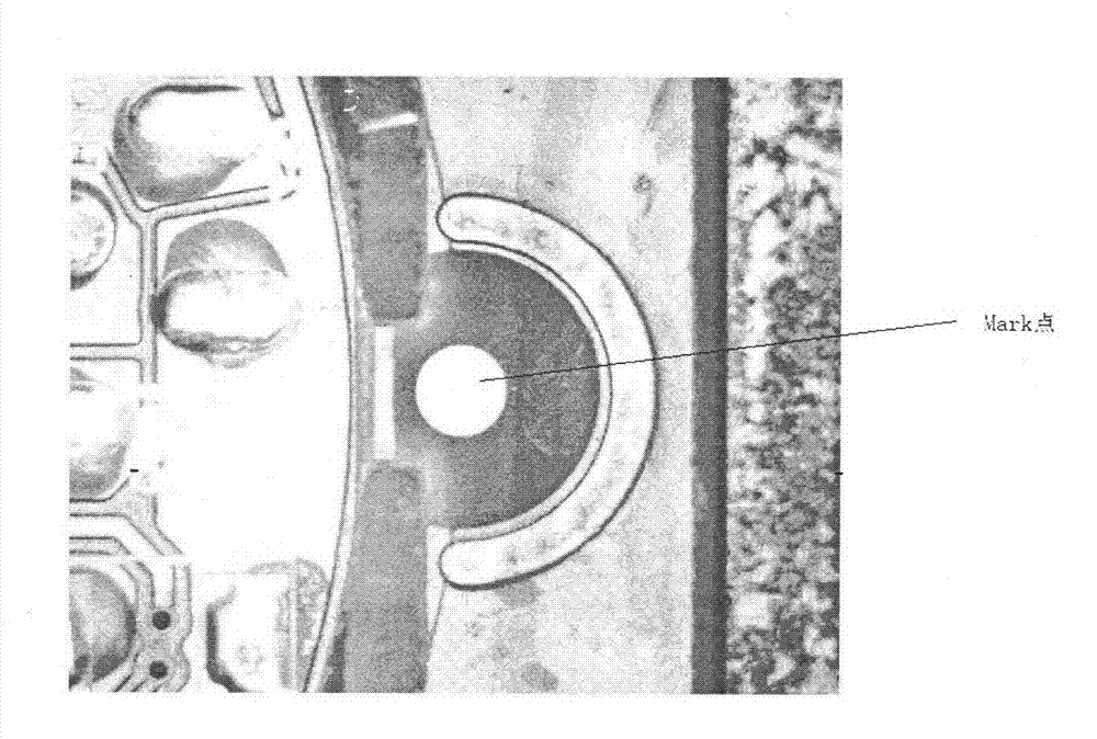
[0018] The image matching method refers to using the Mark point image in the benchmark as a data source. The so-called Mark point image in the benchmark refers to: the Mark point area image cut when doing the program; then when performing automatic detection, Utilize this image to carry out the search of scanning type, when the image size and the shape of finding the image and reference Mark point are all the same, just think that the detected image contains the detection Mark point; The offset between them is used for PCB board compensation.

[0019] The specific operation steps are as follows:

[0020] 1. Use the camera to capture the PCB image containing Mark points, and display it on the computer screen (called FOV field of view, FOV refers to the actual area currently captured by the camera), and then use the screenshot control that co...


PUM


Abstract

The invention discloses a method for positioning Mark points of a PCB (printed circuit board) by image matching. The method is characterized by comprising steps of using a group of Mark point region images shot during programming as reference images; searching by the aid of the images in a scanning manner when detection is carried out; determining that a detected image contains detected Mark points when the size and the shape of the searched image are identical to those of the reference Mark point images; and finally compensating the PCB by deflection among reference Mark points and the detected Mark points. The method has the advantages that comparison is carried out on the basis of image matching, an algorithm and shapes of the Mark points are irrelevant, compensation precision is high, and the problem of inaccurate welding of the PCB due to the fact that the PCB is deflected when the PCB is compensated and then is welded is avoided.

Description

technical field [0001] The invention relates to the field of visual detection of PCB welding, in particular to a method for locating Mark points of PCB boards by using an image matching method, so that the compensation accuracy can be effectively improved when positioning and correcting the PCB boards. Background technique [0002] With the development of computer digital image processing technology and non-destructive testing technology, detection and recognition technology is increasingly developing towards intelligent, high-reliability, high-speed automatic online detection. Computer vision technology and reliability technology are the two major technical foundations of modern inspection. Machine vision has been successfully applied in the field of industrial inspection, which includes automatic detection of PCB boards (ie: printed circuit boards), automatic positioning of circuit boards and calibration of benchmarks, and accurate placement of components in production. D...

Claims


Application Information

Patent Timeline
Patent Type & Authority Applications(China)
IPC IPC(8): B23K1/00
Inventor 廖怀宝
Owner 廖怀宝
Why Eureka
Try Eureka