Optical imaging device and imaging processing method for optical imaging device

An optical image and touch device technology, applied in the direction of electrical digital data processing, data processing input/output process, instruments, etc., can solve the problems of increased manufacturing cost, difficult judgment, difficult assembly, etc., so as to overcome the difficulties in assembly , reduce manufacturing costs, and have the effect of accurate judgment

Inactive Publication Date: 2013-01-16
WISTRON CORP
View PDF7 Cites 5 Cited by
  • Summary
  • Abstract
  • Description
  • Claims
  • Application Information

AI Technical Summary

Problems solved by technology

However, since the reflective frame needs to be coplanar with the sensor, it is difficult to assemble and increases the manufacturing cost; however, an optical image touch device without a reflective frame will be caused by interference sources outside the coordinate detection area. The touch points are difficult to judge due to external interference, so how to design an optical image touch device that can effectively reduce the difficulty and cost of assembly and improve the judgment accuracy of touch points at the same time is the current touch technology. One of the important issues to be worked on

Method used


Image

  • Optical imaging device and imaging processing method for optical imaging device
  • Optical imaging device and imaging processing method for optical imaging device
  • Optical imaging device and imaging processing method for optical imaging device

Examples


Embodiment Construction

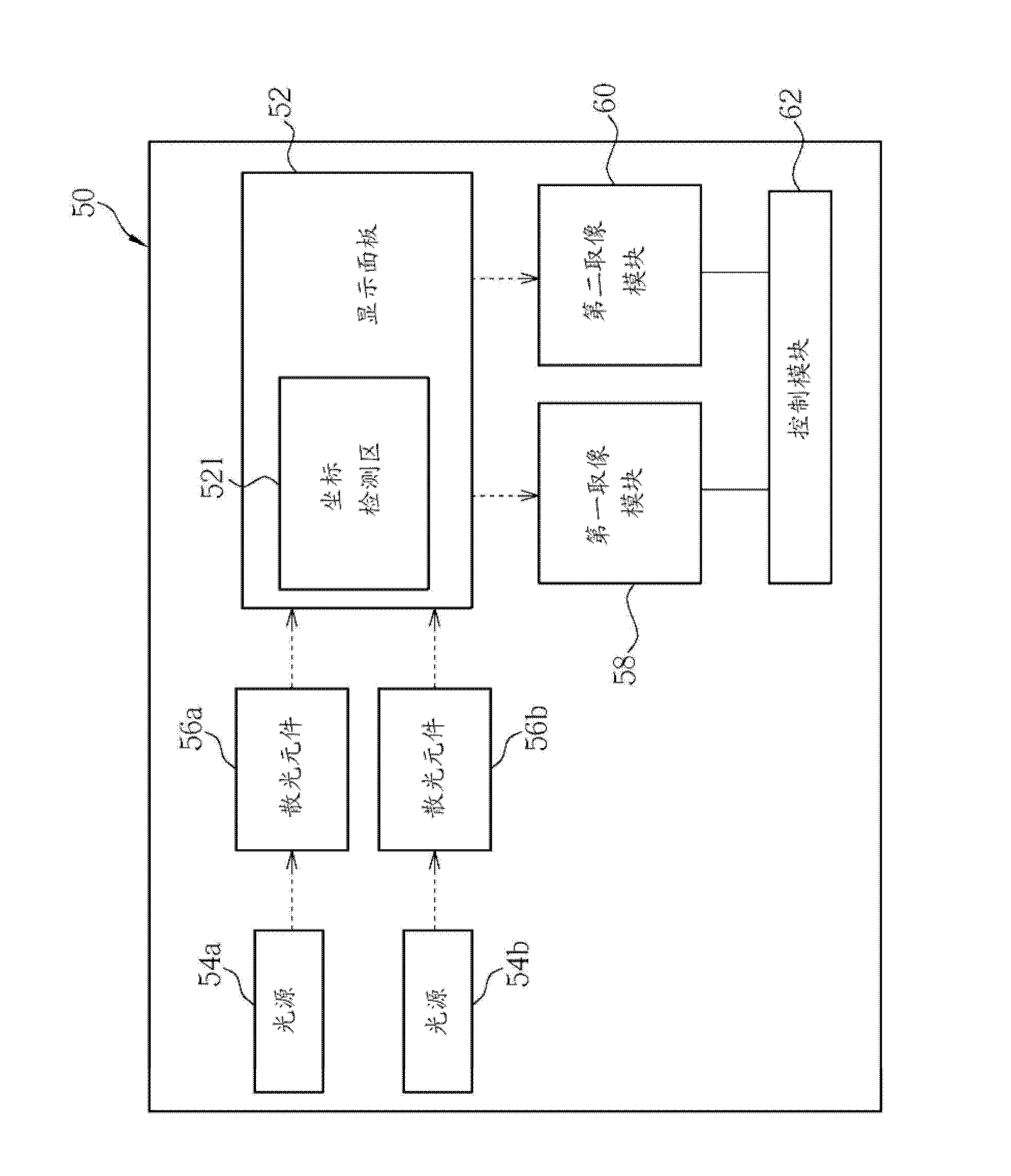
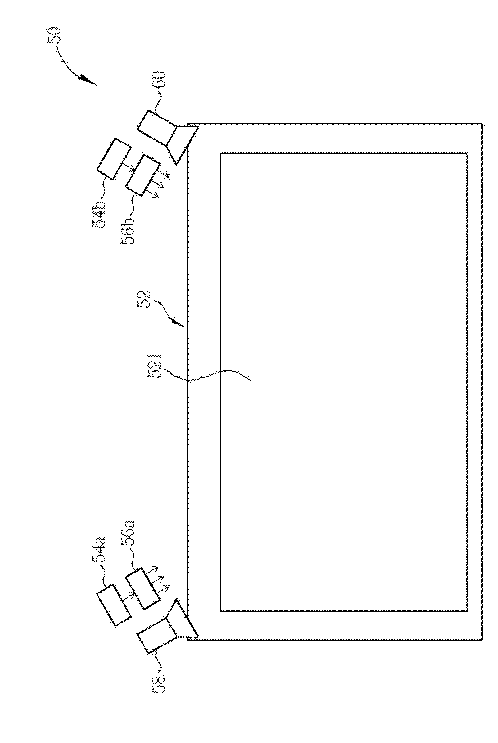
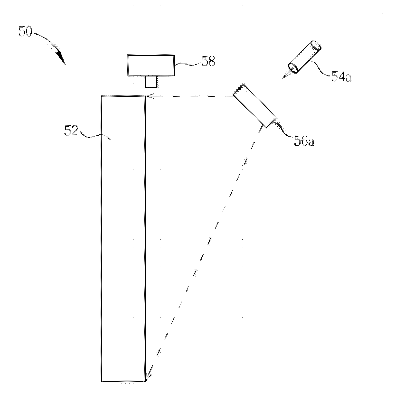
[0033] see Figure 1 to Figure 3 , figure 1 It is a schematic functional block diagram of an optical imaging touch device 50 according to the first embodiment of the present invention, figure 2 and image 3 They are the front view schematic diagram and the side view schematic diagram respectively of the optical image touch device 50 according to the first embodiment of the present invention. A first imaging module 58 , a second imaging module 60 , and a control module 62 . The display panel 52 can be a touch panel, and a coordinate detection area 521 is formed on it; two light sources 54a, 54b are respectively arranged at two corners outside the display panel 52, and the two light sources 54a, 54b are used to emit light to illuminate a object, wherein the two light sources 54a, 54b can be a laser light emitting diode or an infrared light emitting diode, which are used to emit collimated light beams; A linear planar light beam is generated, and the location and quantity of...


PUM


Abstract

An optical imaging device includes a display panel whereon a coordinate detecting area is formed, at least one light source disposed on a corner of the display panel for emitting light to illuminate an object, a first image capturing module disposed on a corner of the display panel for capturing image information of the object, a second image capturing module disposed on another corner of the display panel for capturing image information of the object, and a control module coupled to the first image capturing module and the second image capturing module for determining whether to calculate a coordinate value of the object according to whether the first image capturing module and the second image capturing module capture the image information of the object simultaneously.

Description

technical field [0001] The invention relates to an optical image touch device and a touch image processing method, in particular to an optical image touch device and a touch image processing method without using a reflective frame. Background technique [0002] In today's various consumer electronic product markets, portable electronic products such as personal digital assistants, mobile phones, and mobile phones have widely used touch devices as interface tools for data communication. Since the current design of electronic products is light, thin, short, and small, there is not enough space on the product to accommodate traditional input devices such as keyboards and mice, especially driven by the demand for tablet computers that emphasize humanized design. Displays with touch devices have gradually become one of the key components of various electronic products. However, there are many touch technologies developed today, such as resistive, capacitive, ultrasonic, infrared...

Claims


Application Information

Patent Timeline
Patent Type & Authority Applications(China)
IPC IPC(8): G06F3/042
CPCG06F3/0428
Inventor 陈裕彦黄博亮
Owner WISTRON CORP
Why Eureka
Try Eureka