Liquid crystal display driving method and liquid crystal display

A technology of liquid crystal display and driving method, which is applied in the field of liquid crystal display driving and liquid crystal display, and can solve problems such as insufficient charging of pixel electrodes, influence on display picture quality, and uneven charging of adjacent pixel electrodes, so as to eliminate vertical bright and dark lines and improve image quality. Quality, the effect of improving quality

Inactive Publication Date: 2013-01-16
BEIJING BOE OPTOELECTRONCIS TECH CO LTD
View PDF2 Cites 18 Cited by
  • Summary
  • Abstract
  • Description
  • Claims
  • Application Information

AI Technical Summary

Problems solved by technology

In the existing dual-gate structure LCD driving method, when each frame is displayed, the driving sequence of a pair of gate (Gate) lines corresponding to the same row of pixel electrodes remains unchanged, so that the signal output waveform of the data line And the polarity conversion method, resulting in insufficient charging of the pixel electrodes, making the charging of adjacent pixel electrodes located on both sides of the same data line uneven, so that continuous vertical bright and dark lines appear visually on the screen, seriously affecting the quality of the display screen

Method used


Image

  • Liquid crystal display driving method and liquid crystal display
  • Liquid crystal display driving method and liquid crystal display
  • Liquid crystal display driving method and liquid crystal display

Examples


Embodiment Construction

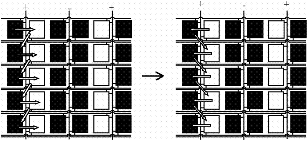
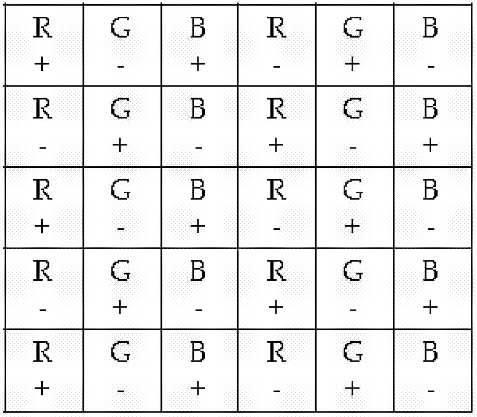
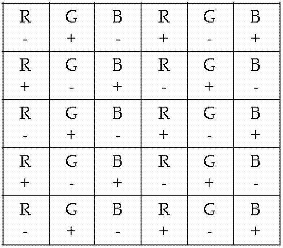
[0024] The liquid crystal display with double-gate structure of the present invention includes a gate drive circuit, a data drive circuit, a plurality of thin film transistors, a plurality of pairs of gate lines, a plurality of data lines and a plurality of pixel electrode groups; wherein, each pair of gate lines includes adjacent An odd-numbered row of gate lines and an even-numbered row of gate lines, each of the pixel electrode groups includes two adjacent pixel electrodes in the same row, and the two pixel electrodes of the same pixel electrode group are connected to the same data line through thin film transistors and respectively connected to different grid lines in a pair of grid lines; pixels arranged in multiple rows and columns are formed on the liquid crystal display, each pixel corresponds to a pixel electrode, and the pixels corresponding to each pixel electrode group are composed of A group of pixels.

[0025] In order to eliminate the phenomenon of vertical brig...


PUM


Abstract

The invention discloses a liquid crystal display driving method and a liquid crystal display. The liquid crystal display comprises a gate driving circuit, a data driving circuit, a plurality of thin film transistors, a plurality of pairs of gate lines, a plurality of data lines and a plurality of pixel electrode groups, wherein each pixel electrode group comprises two adjacent pixel electrodes which are arranged in one same row; the two adjacent pixel electrodes are connected with one same data line and are respectively connected with different gate lines of a pair of gate lines; the liquid crystal display is provided with pixels which are arranged in multiple rows or lines; each pixel corresponds to one pixel electrode; pixels to which each pixel electrode group corresponds are formed as a pixel group. The method comprises the following steps: in a frame of screen, the pixels are driven in accordance with arrangement orders in sequence; when pixels in any row are driven, two pixels of one same pixel group are driven successively and the driving order is alternated and changed in a continuous frame of screens. Therefore, with the adoption of the method, two pixels of one same pixel group corresponding to adjacent pixel electrodes connected with one same data line are charged with power uniformly, so that the screen quality is improved.

Description

technical field [0001] The invention relates to the field of display technology, in particular to a liquid crystal display driving method and a liquid crystal display. Background technique [0002] In recent years, display technology has developed rapidly, and flat panel display devices have the characteristics of complete planarization, light weight, thin thickness, and power saving, which are in line with the development trend of future image display devices. At present, the main flat panel display devices include plasma display panel (Plasma Display Panel, PDP), liquid crystal display (Liquid Crystal Display, LCD), field emission display (Field Emission Display, FED), organic light-emitting diode (Organic Light-Emitting Diode, OELD) ) display devices, etc., among which, LCD is the flat panel display device with the fastest development, the most mature technology and the most widely used. [0003] At present, most LCDs include gate drivers and source drivers, which are us...

Claims


Application Information

Patent Timeline
Patent Type & Authority Applications(China)
IPC IPC(8): G09G3/36
CPCG09G3/3614G09G3/3648G09G2300/0426G09G2310/067G09G2320/0233G02F1/133G09G3/36G09G3/3685
Inventor 孟智明
Owner BEIJING BOE OPTOELECTRONCIS TECH CO LTD
Why Eureka
Try Eureka