Method for manufacturing light emitting diode packaging structure

A technology for light-emitting diodes and packaging structures, applied in electrical components, electrical solid-state devices, circuits, etc., can solve the problems of large thermal resistance between electrodes and substrates, cannot be thinner, and the overall thickness is limited, so as to shorten the conduction path and improve the use of Long life, good heat dissipation effect

Inactive Publication Date: 2013-01-16
ZHANJING TECH SHENZHEN +1
View PDF4 Cites 7 Cited by
  • Summary
  • Abstract
  • Description
  • Claims
  • Application Information

AI Technical Summary

Problems solved by technology

However, today's light-emitting diode elements tend to be more and more light and thin in appearance, and the overall thickness of the light-emitting diode package structure of this structure is limited by the thickness of the substrate and cannot be thinner; in addition, due to the heat generated by the light-emitting diode It is transmitted to the substrate through the electrodes and then radiated outwards. There is usually a large thermal resistance between the electrodes and the substrate, which is not conducive to the heat dissipation of high-power LED lamps.

Method used


Image

  • Method for manufacturing light emitting diode packaging structure
  • Method for manufacturing light emitting diode packaging structure
  • Method for manufacturing light emitting diode packaging structure

Examples


Embodiment Construction

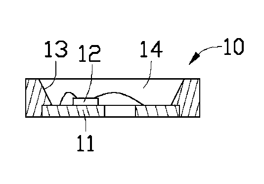
[0021] Such as figure 1 As shown, the light emitting diode package structure 10 provided by the embodiment of the present invention includes two metal layers 11 as electrodes, and a light emitting diode chip 12 installed on one of the metal layers 11 and electrically connected to the two metal layers 11, surrounded by The reflective layer 13 of the LED chip 12 and the encapsulation layer 14 sealing the LED chip 12 .

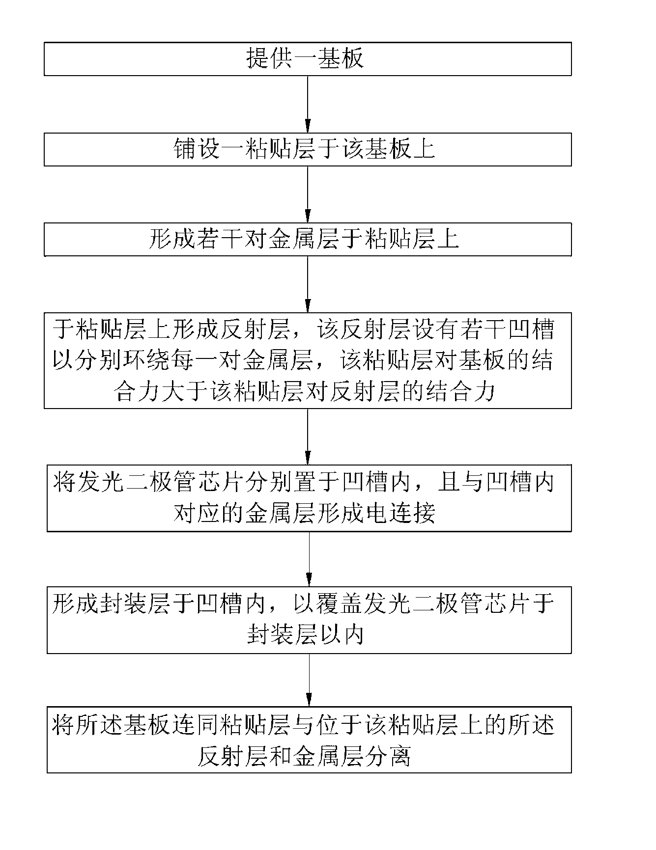
[0022] The present invention also provides a manufacturing method of the above-mentioned light emitting diode packaging structure 10, such as figure 2 As shown, the manufacturing method will be described in detail below in conjunction with other drawings.

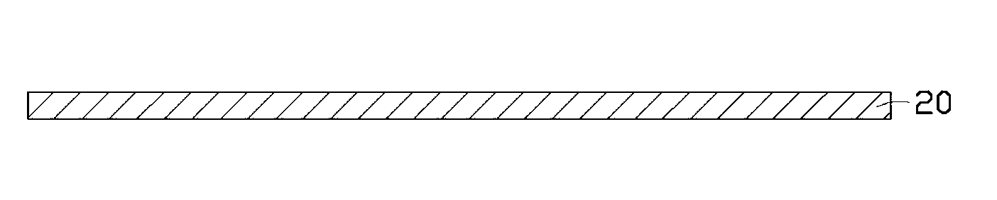
[0023] see image 3 , providing a temporary substrate 20, the temporary substrate 20 is in the shape of a flat plate. The temporary substrate 20 can be made of metal material.

[0024] see Figure 4 , forming an adhesive layer 30 on the upper surface of the temporary substrate 20 , and the adhesive layer...


PUM


Abstract

The invention discloses a method for manufacturing a light emitting diode packaging structure. The method comprises the following steps of: supplying a substrate; paving a sticky layer on the substrate; forming a plurality of pairs of metal layers on the sticky layer; forming a reflection layer on the sticky layer, wherein the reflection layer is provided with a plurality of grooves surrounding the metal layers, and the bonding force of the sticky layer to the substrate is greater than that of the sticky layer to the reflection layer; arranging light emitting diode chips in the grooves respectively, and electrically connecting the light emitting diode chips and corresponding metal layers in the grooves; forming packaging layers in the grooves, and covering the light emitting diode chips in the packaging layers; and separating the substrate together with the sticky layer from the reflection layer and the metal layers which are positioned on the sticky layer. Therefore, the substrate-free light emitting diode packaging structure is formed; the thickness of the light emitting diode packaging structure is reduced; and a thinned structure is realized.

Description

technical field [0001] The invention relates to a semiconductor manufacturing method, in particular to a manufacturing method of a light emitting diode packaging structure. Background technique [0002] Compared with traditional light sources, light emitting diodes (Light Emitting Diode, LED) have the advantages of light weight, small size, low pollution, long life, etc. As a new type of light source, it has been increasingly used in In various fields, such as street lights, traffic lights, signal lights, spotlights and decorative lights. [0003] Existing LED packaging structures generally use a substrate as a packaging substrate, on which electrodes are formed, and LED chips are mounted on the substrate and electrically connected to the electrodes. However, today's light-emitting diode elements tend to be more and more light and thin in appearance, and the overall thickness of the light-emitting diode package structure of this structure is limited by the thickness of the ...

Claims


Application Information

Patent Timeline
Patent Type & Authority Applications(China)
IPC IPC(8): H01L33/00
CPCH01L2933/005H01L33/486H01L33/00H01L2224/48091H01L2224/48247H01L2933/0033H01L2924/00014
Inventor 陈滨全
Owner ZHANJING TECH SHENZHEN
Why Eureka
Try Eureka