Display panel, display device, and drive method therefor

A display panel and display device technology, applied in identification devices, static indicators, optics, etc., can solve the problems of increased current consumption, increased cost and current consumption of display devices, high cost of data signal line drive circuits, etc.

A display panel and display device technology, applied in identification devices, static indicators, optics, etc., can solve the problems of increased current consumption, increased cost and current consumption of display devices, high cost of data signal line drive circuits, etc.

CN102884475AInactive Publication Date: 2013-01-16SHARP KK

Image

  • Display panel, display device, and drive method therefor
  • Display panel, display device, and drive method therefor
  • Display panel, display device, and drive method therefor

Examples


no. 1 Embodiment approach

[0108]

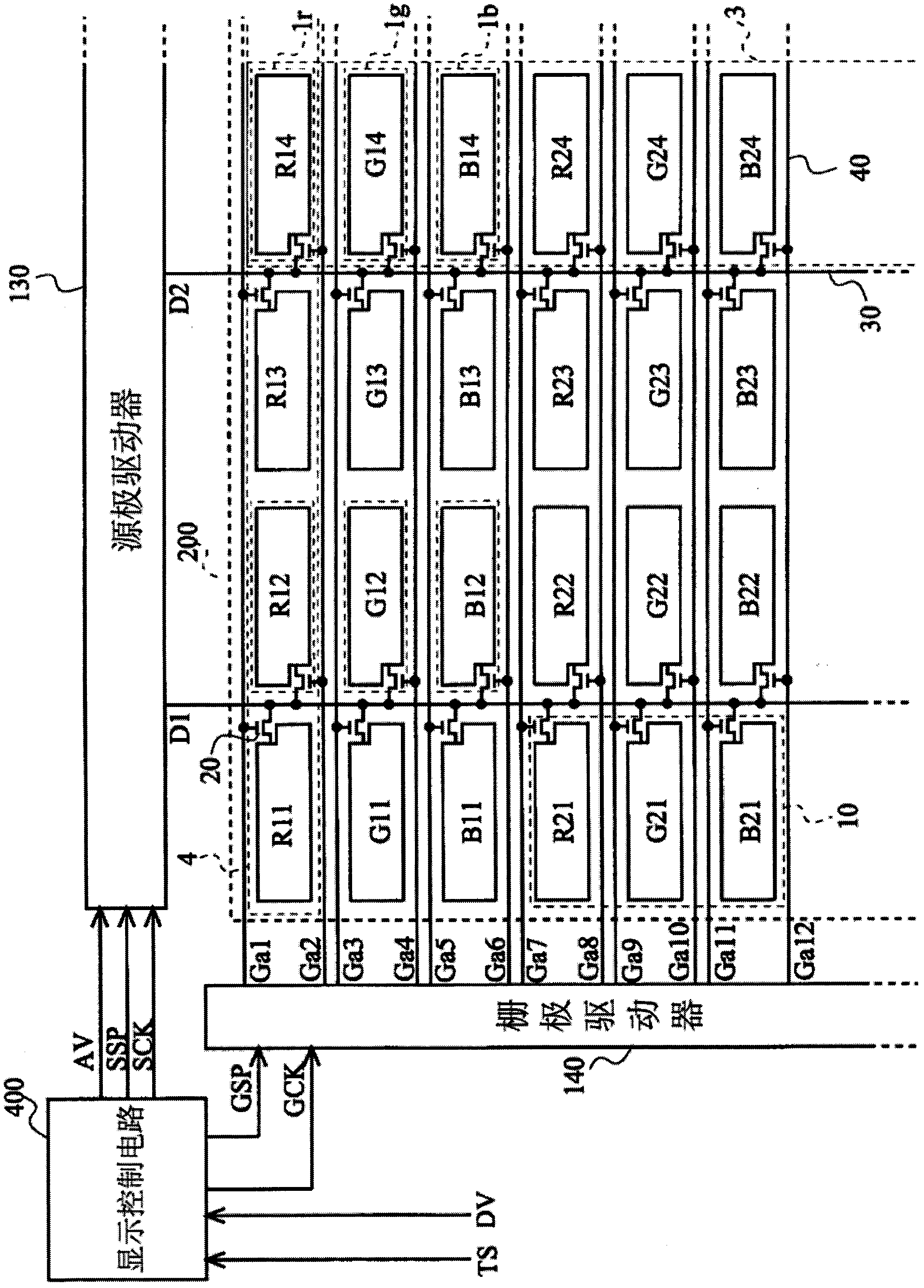
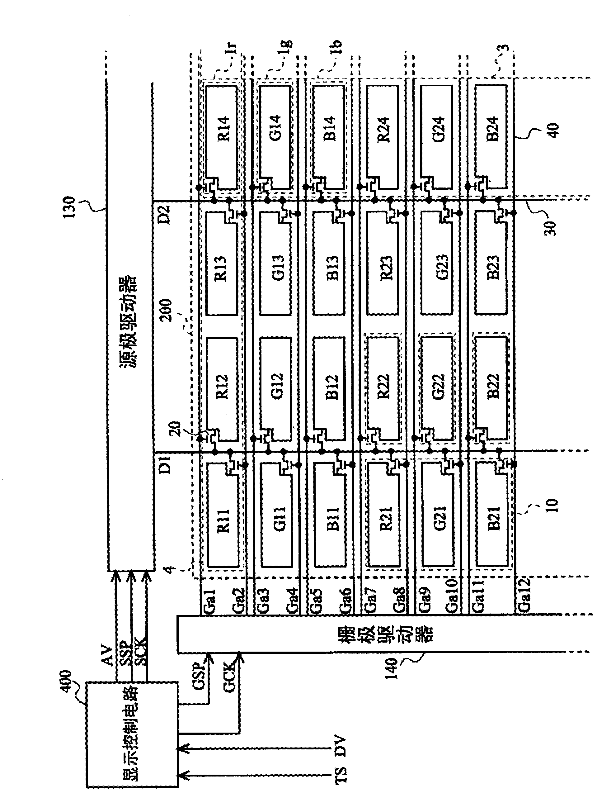
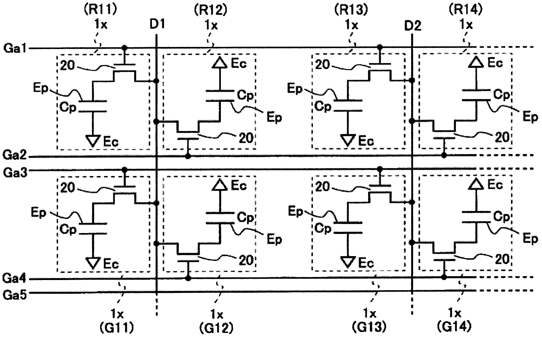
[0109] figure 1 It is a schematic diagram showing the electrical configuration of the liquid crystal display device according to the first embodiment of the present invention. This liquid crystal display device includes: a liquid crystal panel 300 as a display panel; a source driver 130 as a data signal line driving circuit; and a gate driver 140 as a scanning signal line driving circuit. The source driver 130 and the gate driver 140 are connected to the display control circuit 400 . An image signal DV for displaying a color image and a timing control signal TS are input to the display control circuit 400 from outside the apparatus. The liquid crystal panel 300 includes: a plurality of data signal lines 30 connected to the source driver 130 ; and a plurality of scan signal lines 40 connected to the gate driver 140 . The plurality of data signal lines 30 and the plurality of scanning signal lines 40 are arranged to intersect. In addition, the liquid crystal panel...

no. 2 Embodiment approach

[0138] Next, a liquid crystal display device according to a second embodiment of the present invention will be described. The liquid crystal display device of this embodiment basically has the same configuration as that of the above-mentioned first embodiment, but the method of inversion driving and the scanning signals Ga1, Ga2, . . . are different from those of the above-mentioned first embodiment. Therefore, the following description will focus on their differences, and regarding other points, the same reference numerals will be attached to the same or corresponding parts, and detailed description will be omitted.

[0139] Figure 15 (A)~ Figure 15 (C) is a transition diagram of the inversion driving method of this embodiment. Figure 15 (A), Figure 15 (B) and Figure 15 (C) respectively shows the polarity of the data signal Dk acquired by the sub-pixel formation part Xij in the nth frame, the n+1th frame, and the n+2th frame. Each element in the matrix corresponds t...


PUM


Abstract

Provided is a display panel the cost and current consumption of which are reduced by reducing the number of data signal lines compared to conventional ones, a display device provided therewith, and a drive method therefor. Each pixel forming part (10) included in a display unit (200) of a display device is configured by arranging three sub-pixel forming parts (1r, 1g, 1b) for forming sub-pixels respectively having different color components in a data signal line extension direction. Each data signal line (30) is disposed between an odd-numbered sub-pixel forming part vertical column (3) from the front in a scan signal line extension direction and a sub-pixel forming part vertical column (3) adjacent to and behind the odd-numbered sub-pixel forming part vertical column (3) in the scan signal line extension direction. To each data signal line (30), the sub-pixel forming part vertical columns (3, 3) located on both sides thereof are connected. Each scan signal line (40) is disposed on both sides of the sub-pixel forming part in the data signal line extension direction. The sub-pixel forming part vertical columns (3, 3) adjacent to each other are connected to the scan signal lines (40) different from each other.

Description

technical field [0001] The present invention relates to an active matrix display panel, a display device equipped with it, and a driving method thereof. Background technique [0002] Generally, a display portion of a display panel of an active matrix display device includes pixel forming portions arranged in a matrix. The pixel forming portion has a plurality of sub-pixel forming portions. For example, in an active matrix display device that displays a color image based on the three primary colors of R (red), G (green), and B (blue), conventionally, three sub-pixels for R, G, and B are formed. Three sub-pixel forming portions are arranged in a direction in which the scanning signal lines extend to constitute one pixel forming portion. Figure 18 It is a schematic diagram showing the electrical configuration of main parts of such a conventional active matrix display device. This display device includes a display unit 200 , a data signal line drive circuit 130 , and a scan s...

Claims


Application Information

Patent Timeline
16 Jan 2013
Publication
CN102884475A
IPC
G02F1/133; G02F1/1343; G02F1/1368; G09F9/30; G09G3/20; G09G3/36
CPC
G09G2300/0439; G02F1/136286; G09G3/3614; G09G3/3648; G02F1/133; G09G2300/0426
Inventors
岩本明久; 森井秀树